TI adds PMBus control interface to buck converters

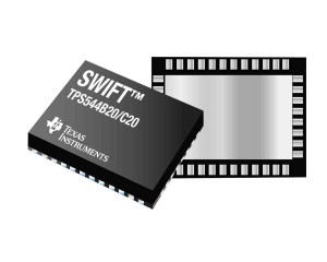
TPS544B20 Texas Instruments has introduced its first 18V, 20A and 30A synchronous DC/DC buck converters with a PMBus digital power control interface.

The SWIFT TPS544B20 and TPS544C20 converters also have integrated MOSFETs.

The reference voltage accuracy is specified at 0.5% and there is differential remote voltage sensing for powering processor-based SoCs.

Selectable D-CAP or D-CAP2 adaptive on-time control mode is designed to provide a fast load transient response and reduces external component count.

The PMBus is used for programming, real-time monitoring of the output voltage, current and external temperature and fault reporting.

For PMBus applications without output voltage, current and board temperature telemetry, TI offers the 12A SWIFT TPS53915 buck converter.


Raspberry Pi gets the kit for industrial prototyping

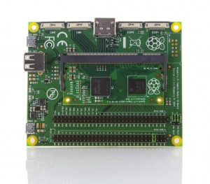
Raspberry Pi Compute Module IO board

Raspberry Pi Compute Module IO board

Raspberry Pi is being re-invented as a prototyping board for commercial embedded designs which will eventually be shipped in volume as products.

The recently introduced Raspberry Pi Compute module is intended to expand the use of the low cost embedded computer outside of its traditional use as an educational teaching aid.

The so-called professional design environment is an area of the market where Raspberry Pi has struggled to compete with established boards such as Arduino and Beagle bone.

“With significant interest in using the Raspberry Pi in industrial and embedded applications the logical next step is to provide engineers with all the benefits the traditional board in a flexible form factor to support embedded design, hence the development of the Raspberry Pi Compute Module,” said Raspberry Pi supplier element14, and the distributor has introduced a development kit for the new module.

The aim has been to create a computer platform with the features of a embedded development system.  The module’s BCM2835 CPU has 512Mbyte RAM with an on board 4Gbyte eMMC flash memory for booting the Linux OS.

With the kit comes a functional IO board which supports an extensive GPIO and multiple connectors to provide access to all of the BCM2835 functionality.

Raspberry Pi Compute Module is a SODIMM sized 6.5cm x 3cm board with 200-pin edge connector

The IO board has multiple GPIO interfaces: 1 x micro USB connector type B, 1 x USB connector type A, 2 x CSI ports for camera boards, 2 x DSI ports for display boards and Full size HDMI port.

“We expect the Raspberry Pi Compute Development Kit to be adopted by design engineers for industrial applications making the power of Pi accessible to more than just the hobbyist,” said Claire Doyle, Global Head of Raspberry Pi, element14.

The Compute Development Kit costs $200 and is available from Farnell element14 and CPC in Europe, Newark element14 and MCM in North America and element14 in APAC.

Harvard measures graphene mass

Researchers at Harvard School of Engineering have observed that graphene electrons exhibit mass when they move together, although they are individually mass-less.

Professor Donhee Ham and Dr Hosang Yoon have successfully measured the collective mass of ‘massless’ electrons in motion in graphene.

By shedding light on the fundamental kinetic properties of electrons in graphene, this research may also provide a basis for the creation of circuits with graphene-based components.

“Graphene is a unique material because, effectively, individual graphene electrons act as though they have no mass. What that means is that the individual electrons always move at a constant velocity,” explains Ham. “But suppose we apply a force, like an electric field. The velocity of the individual electrons still remains constant, but collectively, they accelerate and their total energy increases—just like entities with mass. It’s quite interesting.”

Without this mass, the field of graphene plasmonics cannot work, so Ham’s team knew it had to be there—but until now, no one had accurately measured it.

“One of the greatest contributions of this work is that it is actually an extremely difficult measurement,” says Ham.

As Newton’s second law dictates, a force applied to a mass must generate acceleration. Yoon and Ham knew that if they could apply an electric field to a graphene sample and measure the electrons’ resulting collective acceleration, they could then use that data to calculate the collective mass.

But the graphene samples used in past experiments were replete with imperfections and impurities—places where a carbon atom was missing or had been replaced by something different. In those past experiments, electrons would accelerate but very quickly scatter as they collided with the impurities and imperfections.

“The scattering time was so short in those studies that you could never see the acceleration directly,” says Ham.

To overcome the scattering problem, several smart changes were necessary.

The team was able to reduce the number of impurities and imperfections by sandwiching the graphene between layers of hexagonal boron nitride, an insulating material with a similar atomic structure, and by designing a better way to connect electrical signal lines to the sandwiched graphene.

Yoon and Ham applied an electric field at a microwave frequency, which allows for the direct measurement of the electrons’ collective acceleration in the form of a phase delay in the current.

“By doing all this, we translated the situation from completely impossible to being at the verge of either seeing the acceleration or not,” says Ham. “However, the difficulty was still very daunting, and Hosang made it all possible by performing very fine and subtle microwave engineering and measurements—a formidable piece of experimentation.”

Collective mass is a key aspect of explaining plasmonic behaviors in graphene. By demonstrating that graphene electrons exhibit a collective mass and by measuring its value accurately, Yoon says, “We think it will help people to understand and design more sophisticated plasmonic devices with graphene.”

The challenge remains to improve the quality of graphene samples so that the detrimental effects of electron scattering can be further reduced.
Toshiba brings lithium-titanate battery to UK grid.

Toshiba will provide the battery for the UK’s first 2MW scale lithium-titanate battery based Energy Storage System (ESS) to support grid management. Toshiba’s 1MWh SCiB battery will be installed in a primary substation in September.

Large-scale ESS are increasingly seen as a versatile solution in managing electricity supply. Installed in wind and photovoltaic generation systems, ESS can help to overcome intermittent output and frequency fluctuations, as well as performing peak power buffering, and when connected to the grid they can support grid stability and reinforcement.

This role in grid management will be investigated in the UK, in the Grid Connected Energy Storage Research Demonstrator project, led by the University of Sheffield, funded by the Engineering and Physical Sciences Research Council (EPSRC), with support from both industrial and academic partners.

The ESS will be connected to the 11kV grid at Western Power Distribution’s Willenhall primary substation, near Wolverhampton in the West Midlands. When the project starts operation in November this year, it will allow testing at realistic levels, and allow assessment of both the technical and economic potential of ESS in the grid.

Toshiba’s SCi is a lithium-titanate based secondary battery capable of over 10,000 charge-discharge cycles with and aclow risk of fire – a danger associated with other lithium-ion batteries.

Micron moves towards TLC and 3D NAND

Micron had revenue of $3.98 billion and net income of $806 million for the three months to the end of May. It expects $4 billion to $4.2 billion revenues in the current quarter.

Gross margin was 34% and free cash flow was $880 million based on operating cash flow of $1.46 billion less capex of $576 million

Although Micron says that demand is growing for all its products, it is not planning to build new fabs.

“Driven by a slowing rate of technology migration, supply bit growth trends have stabilised at a level below historical average,” says CEO Mark Durcan, “there appear to be only limited additions of new wafer capacity on the horizon

In the case of NAND, there is not much point building fabs for planar NAND when 3D NAND, which requires a different tool-set to planar NAND, is on the way.

Micron is cagey about its introduction of 3D NAND. “We have said that we believe that this is going to be a material impact on the industry in the second half of 2015,” says Durcan.

The likely last generation of planar NAND will be the 16nm generation where Micron has been struggling to get a triple level cell (TLC) memory to market.

“We are aggressively working on our development of our 16-nanometer TLC roadmap in an effort to drive our overall NAND cost competitiveness,” says Micron president Mark Adams, “we expect to see component samples of our 16-nanometer TLC by the end of calendar year with client-based TLC SSD by spring of 2015.”

Micron anticipates its ‘termination benefits’ cost – mainly for the Italian researchers’ job losses – to be in the region of $15 million to $25 million.

Xilinx and Pico Computing provide Hybrid Memory Cube interface for 20nm FPGAs.

Xilinx, and Pico Computing have made available now a 15Gb/s Hybrid Memory Cube (HMC) interface for All Programmable UltraScale devices.

The Xilinx UltraScale devices support the HMC bandwidth of 4 lanes, comprised of 64 transceivers running up to 15Gb/s.

Pico Computing’s HMC controller IP offers high memory bandwidth.

“Customers can now leverage the industry’s only shipping 20nm FPGAs along with a validated IP core to bring their 15Gb/s HMC designs to market today,” says Xilinx’s Tamara Schmitz, “UltraScale FPGAs are the only devices currently available that can support all four HMC lanes to enable full memory bandwidth with additional transceivers for datapath and control signals.”

Altera’s Interlaced Look-Aside core compatible with Cavium’s NEURON.

Altera’s Interlaced Look-Aside intellectual property (IP) core has been is compatible with Cavium’s NEURON Search Processor and is available now.

The core provides networking OEMs with a packet interface for use in routers, switches, firewalls, and security storage.

The core is integrated in Altera’s Arria 10 and Stratix V FPGAs and enables interoperability between a datapath device and a look-aside coprocessor with transfer rates up to 300 Gbps delivering 500 million packets per second performance.

The core has both soft and hardened logic blocks offering lane and data rate configuration flexibility for optimal integration.

Altera and Cavium tested and verified the Core using a Stratix V FPGA and a NEURON Search Processor.

An interoperability report is available from Altera that describes the testing methods and performance metrics achieved using Altera’s Interlaken Look-Aside IP core interfacing with Cavium’s NEURON Search Processor.

Intel and Microsoft in London for signage forum

intelArrow Electronics is running a Digital Signage Forum for original equipment manufacturers (OEMs) and system integrators which is taking place on Wednesday, July 2nd in London.

Arrow said the event will include Intel, Kontron, Microsoft, 3M and Dell. 

Independent digital agency Smart Cookie will deliver a keynote address, while Dell will feature Tobii Glasses 2 – the New Generation Wearable Eye Tracker.

Participants who register online will also receive Arrow’s free white paper “Digital Signage: a communications solution for the new buying experience”.

According to Amir Mobayen, general manager, Arrow OEM computing solutions EMEA,  one reason for holding this event now is that customers’ expectations today are vastly different with online, in-store and mail interactions now ubiquitous.

To register for the Digital Signage Forum.

Government to address flaky mobile telecoms service

The Prime Minister has joined the rest of us in getting fed up with ‘not-spots’ – areas where you can’t get a mobile phone signal.

Astonishingly, it appears, that even Downing Street suffers from flaky mobile service while, it is said that the PM has had to cut short West Country holidays because of lack of a mobile signal.

But relief may be at hand, not only for the PM, but for the rest of use.

The plan is to tell network operators to make their masts accessible to all users.

So your mobile phone gets connected to the nearest mobile mast whoever it belongs to.

The operators, of course, are against the plan. They say switching between different operators’ masts will itself caused dropped calls.

The minister charged with the task of bringing the operators round to the PM’s way of thinking is culture secretary Sajid Javid.

The EU moves to provide free roaming in 2016 have, apparently, precipitated the UK plan because the EU plan would mean that visitors to the UK would get a better service than the locals who would remain tied to one operator’s network.

Raspberry Pi can be image recognition system

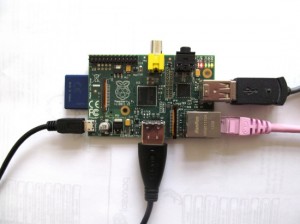
Raspberry Pi

Raspberry Pi

A US-based start-up has come up with a way to port its image recognition software development kit (SDK) to the Raspberry Pi.

“This because it shows that even tiny, cheap devices are capable of performing sophisticated computer vision tasks,” said Pete Warden, chief technology officer at Jetpac.

“This is a tangible example of how object detection is going to be commoditized and ubiquitous,” said Warden.

Possible  applications include detecting endangered wildlife, traffic analysis, satellites, even intelligent toys.

Raspberry Pi has the capability, due to its embedded GPU for heavy lifting on the math side, to process a frame in around three seconds.

Warden took advantage of having access to the assembler level code of the Raspberry Pi processor from Broadcom and has written custom assembler programs for the Pi’s 12 parallel ‘QPU’ processors.

“Broadcom only released the technical specs for their graphics chip in the last few months, and it’s taken a community effort to turn that into a usable set of examples and compilers,” said Warden.

“I ended up heavily patching one of the available assemblers to support more instructions, and created a set of helper macros for programming the DMA controller, so I’ve released those all as open source,” said Warden.

He believes more manufacturers could follow Broadcom’s lead and give access to their GPUs at the assembler level.

“There’s a lot of power in those chips but it’s so hard to tune algorithms to make use of them without being able to see how they work,” said Warden.

Download the library.