Quantum transmission sent through space

The first quantum transmission to go via space paves the way for ultra-secure communications satellites.

Secret encryption keys transmitted via quantum links provide the ultimate way to communicate securely. That’s because any attempt to intercept the key will be revealed thanks to the laws of quantum mechanics, which say that interception will introduce changes that give away eavesdroppers.

The technology is already available for fibre-optic cables, but a truly global network would need satellites to beam quantum data between distant locations. To test how these might work, Paolo Villoresi at the University of Padua in Italy and his colleagues turned to satellites covered in ultra-reflective mirrors. These are normally used to bounce laser beams back to Earth. The time they take to return shows up any shifts in gravity.

In 2007, the team sent a beam of light to space using the Matera Laser Ranging Observatory (MLRO) in Italy and detected single photons bounced off Japan’s Ajisai satellite. For the latest experiment, they prepared photons in four different quantum states – the minimum required to generate an encryption key – and sent them to space using the MLRO. They were able to receive quantum bits of information, or qubits, bounced back from five satellites up to 2600 kilometres above. That smashes the previous record for sending quantum information – 144 kilometres, between two locations on Earth.

To ensure they didn’t count background photons that were not part of the signal, the team timed the laser pulses exactly, rejecting any light that returned outside a narrow time window. The observatory acted as the transmitter and receiver, so the team decided not to send an encrypted message. Still, the team thinks the photons would have been able to encrypt about one bit of data a second.

The team has a way to go before quantum satellites are up to speed. Light travells easily through fibre optic cables compared to turbulent air, so ground-based commercial versions of the technology can encrypt at much faster rates of at least 1 megabit a second.

Villoresi compares the performance to Sputnik, the first-ever satellite, launched in 1957. “Comments at the time were, ‘How nice, the satellite can send a few beeps, it’s totally useless’,” he says. “We are more or less the same level.” But even a very limited data channel could be used to send secure commands to a spacecraft, he says.

Rupert Ursin at the Institute for Quantum Optics and Quantum Information in Vienna, Austria, points out that Villoresi’s team sent the qubits in four bursts, each tens of seconds apart. That means they did not detect all four quantum states at once, which would be necessary for a true quantum satellite.

And Jian-Wei Pan at the University of Science and Technology of China in Hefei notes that a lot of photons are lost in transmission, so he is not sure the signal would be strong enough to transmit a full quantum key. But Pan and Ursin both say the work shows the technology is getting close.

China has announced plans to launch a true quantum communications satellite in 2016, and other nations’ space agencies are investigating the possibility. “Everything is ready, and if we had enough money we could fly,” says Ursin. “The risk that we fail in space is reduced thanks to these kinds of experiments.”

Journal reference: arxiv.org/abs/1406.4051

Syndicated content: Jacob Aron, New Scientist 

Silicon Labs adds to capacitive sensing MCUs

Silicon Labs C8051F97x - block diagram

Silicon Labs C8051F97x – block diagram

Silicon Labs is sampling capacitive sensing microcontrollers (MCUs) for human-machine interfaces (HMI).

The C8051F97x MCU is for Internet of Things, home/building automation, consumer and industrial markets.

It targets battery-powered and capacitive touch sensing applications for handheld industrial devices, toys, gaming machines and remote controls, as well as touch-panel switch replacements for white goods such as washers, dryers, ovens and dishwashers.

The MCUs draw 200 µA/MHz active current, a two-microsecond wake time and a sleep mode energy consumption of 55 nA with brownout detector enabled and 280 nA sleep current with a 16.4 kHz internal oscillator.

They incorporate Silicon Labs’ SAR charge-timing capacitance-to-digital converter (CDC) technology which has 40 microsecond acquisition time.

Silicon Labs’ CDC technology offers superior noise immunity for reliable performance in challenging conditions and configurations such as thick laminate overlays, electrical noise or variances in printed circuit board (PCB) manufacturing.

This CDC hardware implementation is capable of measuring capacitance on a wide range of materials including PCBs, flex circuits, and indium tin oxide (ITO) on glass and film.

The F97x MCU family expands the capabilities of Silicon Labs’ C8051F99x low-power capacitive sensing MCUs with up to 43 capacitive sensing inputs, 32 kB flash memory, 8 kB RAM, seven DMA channels and a 16 x 16 multiply-accumulate (MAC) unit in QFN packages as small as 4 mm x 4 mm. The F97x MCUs integrate a 25 MHz pipelined 8051-compatible core, a precision oscillator, a 10-bit analog-to-digital converter (ADC), a temperature sensor, a voltage reference and four 16-bit general-purpose timer/counters.

Linear retunes low noise fractional-N PLL

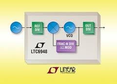
Linear Tech Linear Technology has introduced a fractional-N phase-locked loop (PLL) with 6GHz-plus integrated voltage-controlled oscillator (VCO).

The LTC6948 has a fourth order delta-sigma modulator that employs noise-shaping techniques to minimise noise contribution without creating the fractionalisation spurs typically found with fractional-N PLLs.

The chip is a fractional-N PLL with integer-N spurious performance.

The benefits of fractionalisation are frequency agility and improved phase noise.

The device has a -274dBc/Hz normalised 1/f noise specification that does not affect its -226dBc/Hz normalised in-band phase noise floor.

Typical applications include wireless communications using complex modulation schemes, communications systems that employ long burst durations and Doppler radar.

There are four versions of the LTC6948, each offering a different VCO frequency band with the fastest option delivering up to 6.39GHz.

The VCO output divider can be programmed from 1 through 6 to cover a wide range of frequencies down to 373MHz. V  

The FracNWizard simulation and design tool is available for free download.

All versions of the LTC6948 are specified over the full operating junction temperature range from -40°C to 105°C. The products are available in a 4mm x 5mm, 28-lead plastic QFN package.


ST’s audio chip goes from soft to LOUD

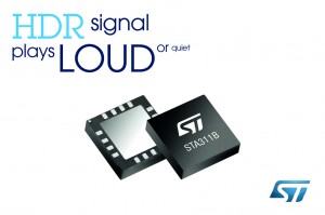
STSTMicroelectronics’ latest audio processor has been designed with a wide dynamic range which allows digital signals with a dynamic range exceeding 130dB to be generated without the need for high-performance ADCs (analogue-to-digital converters).

The STA311B embeds eight audio-processing channels with up to 10 independent user-selectable bi-quadratic filters per channel, input and output mixing capabilities with multi-band dynamic range compression.

There is also auto-detection of input sampling frequency, input and output RMS metering, and pulse width modulation technology.

The input/output RMS metering function is designed to deliver an increased level of safety to the final product without any additional hardware cost.

This allows the application to suppress unwanted energy surges that could potentially damage the speakers.

The STA311B’s pop-free circuitry also enables a seamless start-up, eliminating unwanted noise due to the bridge charge sequence in both Single-End and Bridge-Tied Load configurations.

The device is available in a 8.0×8.0×0.9mm VFQFPN package,

The STA311B is supported by ST’s free APWorkbench software development tool.


Infineon expands Villach

Infineon - Peter Schiefer

Infineon Head of Operations – Peter Schiefer

Infineon is expanding its Austrian site in Villach in a project it calls “Pilot Space Industry 4.0”.

This, says Infineon, is an ‘ innovative concept for networked and knowledge-intensive production’.

Research on new materials and technologies will also be intensified.

Infineon’s expansion plans foresee investments and research costs amounting to a total of € 290 million, creating approximately 200 new jobs in the period from 2014 to 2017, primarily in R&D.

infineon’s Peter Schiefer, Says: “The continuing development of Villach is a part of our group-wide manufacturing strategy. At the site, important developments will be advanced and production-ready innovative technologies will be transferred by Infineon to other sites. At the same time our strategy will include expansion of our volume manufacturing on 300 millimeter thin wafers in Dresden and on 200 millimeter wafers in Kulim, Malaysia.”

Sabine Herlitschka, CEO of Infineon Austria, says: “With the expansion concept Villach is reinforcing its important role as a factory of innovation and a competence center for power electronics within the corporate group. We’re coupling the innovation factory in Villach with volume production in Dresden using the example of 300 millimeter thin wafer production for power semiconductors.”

Infineon will construct a complex for research, production and measurement technology workstations.

Logistics, miscellaneous infrastructures and the plant equipment will also be expanded to meet future demand. This will let Infineon mobilize the productivity and automation called for in international competition, while at the same time increasing flexibility.

Infineon has been actively engaged in the Industry 4.0 initiative from the very beginning; its pilot space in Villach is another step towards realising it.

A wide-scale research program with innovations in materials, processes, technologies and system expertise is the second pillar of the Villach site expansion, supporting development of the next generation of energy-efficient products.

Here the program focuses on the integration of innovative substrates such as gallium nitride and silicon carbide, on MEMS (Micro-Electro-Mechanical Systems) and sensor technologies as well as on the continuing development of 300 millimeter thin wafer technology.

Spansion adds to auto micros

Spansion Traveo automotive microcontroller S6J3100 series

Spansion Traveo automotive microcontroller S6J3100 series

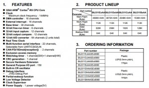
Spansion is sampling its Traveo automotive microcontroller S6J3100 series with a CAN FD interface for in-vehicle networking.

The chip,is for various automotive applications including body control module (BCM), heating, ventilation and air conditioning (HVAC).

Bosch invented the CAN standard many years ago and since then worked to improve in-vehicle communication through innovative solutions. Bosch introduced CAN FD as a seamless upgrade of the classic CAN technology the first time at the International CAN Conference in 2012. Like classic CAN, CAN FD enables highly reliable vehicle control, taking advantage of higher data rates with only a small impact on current software and applications. Spansion has started to supply MCU products equipped with CAN FD.

As well as In the CAD FD interface operating at 5Mbps, the S6J3110 series comes with a maximum 4MB of flash memory and uses 55nm technology. It has Secure Hardware Extension (SHE) for network security and improved performance for connected cars, and partial wakeup for lowering power consumption.

The Spansion Traveo family of microcontrollers is based on the ARM Cortex-R5 core and tailored for a broad range of automotive applications.

In May 2014, Spansion introduced the first product of the family, the MB9D560 series for vehicle electrification utilised in hybrid electric vehicles (HEV) and electrical vehicles (EV).

TSMC full for the rest of the year

TSMC will run at 100% fab utilisation throughout the second half of the year, reports Digitimes.

Digitimes is quoting Morris Chang who also said that 20nm would account for 10% of total revenues in Q3 and 20% in Q4.

45nm and better processes account for half total revenues.

TSMC says it has 20 customers for its 16nm finfet process.

The company says it will set up a 300-400 person R&D lab to develop a 10nm process scheduled for trial production in 2015 and mass production in 2016.

Total capacity in 2013 was 15.67 million eight inch wafer equivalents. In 2012, it was 14.04 million.

AMS and Dialog in merger talks

AMS - DialogA new European semiconductor IDM could be on the cards if talks between AMS, the former Austria Micro Systems, and Dialog bear fruit.

Merger talks are underway between specialised foundry AMS and Dialog with AMS needing to make an offer for Dialog by July 24th if the acquisition is to happen.

AMS says: ‘AMS and Dialog confirm that the two companies are in preliminary discussions regarding a possible merger of equals of AMS and Dialog Semiconductor. These discussions are at a very preliminary stage and there can be no certainty that a transaction will be forthcoming.’

AMS had revenues of $502 million last year and has a market cap of $2.3 billion while Dialog had revenues of $903 million last year and has a market cap of $1.8 billion.


Technologists honoured in Queen’s Birthday List

Professor Thomas Walter Bannerman Kibble - Imperial

Professor Thomas Walter Bannerman Kibble – Imperial

The Queen’s Birthday Honours included knighthoods for Professor Thomas Walter Bannerman Kibble, CBE FRS Senior Research Fellow and Emeritus  Professor of Theoretical Physics at  Imperial College London, for services to Physics, and  Professor John Bernard Pethica, FRS FREng, Chief Scientific Adviser, National Physical Laboratory and Physical Secretary and Vice-President of The Royal Society for services to Science.

Dr Pamela Louise Makin, CEO BTG, becomes a Dame for the Life Sciences Industry.

The CBE goes to David James Gow, Inventor, I-Limb Hand, for services to Upper Limb Prosthetics.

The OBE goes to: Alexander David Beatty, Vice-President, Advanced Weapon Systems, Thales for services to the Aerospace and Defence Industries in  Northern Ireland; Dr Paul Martin Hawkins,  Managing Director and Chairman, Hawk-Eye  Innovations for services to Technology and Sport;  Dr Helen Elizabeth Mason,  Reader in Solar Physics, University of  Cambridge, for services to Higher  Education and to Women in Science, Engineering and Technology; Anupam Ojha,  Director, National Space Academy, for services to Science Education and Ms Belinda Parmar, CEO  Lady Geek for services to Women in Technology.

The MBE goes to: Dr Robert Samuel Andrews, Commercial Director, EW Simulation Technology,  for services to the Defence Industry; Professor William David Evans,  Consultant Physicist and Head of Medical Physics and Clinical Engineering, Cardiff and Vale University Health Board, for services to the NHS in Wales and Overseas, Mary Margaret, Grant Head of Science, Newry High School, for services to Education and to the community in Northern Ireland;  James Walker Kane Chairman, J W Kane Engineering,  for services to the Aerospace Industry in Northern Ireland; Professor Colin Robert McInnes, FREng FRSE Director, Advanced Space Concepts Laboratory, for services to Space Research, Science and Technology; Robert Joseph Schukai, Global Head, Mobile Technologies, Thomson Reuters for services to British trade and investment and to promoting STEM education.

Image: Imperial College - Professor Thomas Walter Bannerman Kibble

Microchip adds data encryption to PIC microcontrollers

microchipMicrochip has tuned its eXtreme Low Power (XLP) PIC microcontroller range with increased data protection capabilities.

The MCUs integrate a hardware crypto engine, a Random Number Generator (RNG) and One-Time-Programmable (OTP) key storage  or protecting data in embedded applications.

Several security features are integrated into the PIC24F “GB2” family, to protect embedded data. The fully featured hardware crypto engine, supporting the AES, DES and 3DES standards, reduces software overhead, lowers power consumption and enables faster throughput.

The PIC24F “GB2” devices offer up to 128kbyte flash and 8kbyte RAM in small 28- or 44-pin packages, for battery-operated or portable applications.

A Random Number Generator creates random keys for data encryption, decryption and authentication, to provide a higher level of security.
For additional protection, the One-Time-Programmable (OTP) key storage prevents the encryption key from being read or overwritten.

These security features increase the integrity of embedded data without sacrificing power consumption. With XLP technology, the “GB2” family achieves 180 µA/MHz Run currents and 18 nA Sleep currents, for very long battery life in portable applications.

The MCUs also integrate USB for device or host connections, as well as a UART with ISO7816 support, which is intended for smartcard applications.  

Product variants are available with USB (PIC24FJXXXGB2XX) and without USB (PIC24FJXXXGA2XX). The PIC24FJ128GB204, PIC24FJ64GB204, PIC24FJ128GA204 and PIC24FJ64GA204 are offered in 44-pin TQFP and QFN packages. The PIC24FJ128GB202, PIC24FJ64GB202, PIC24FJ128GA202 and PIC24FJ64GA202 are available in 28-pin SOIC, SSOP, SPDIP and QFN packages. All of these new MCUs are available today for sampling and volume production.