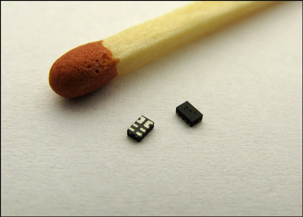
Silego launches load switch

Silego SLG59M1563V

Silego SLG59M1563V

Silego has introduced another member of its GreenFET3 load switch product line. The SLG59M1563V has an RDSON of 22.5 mΩ. It supports up to 2.5 A continuous current, reverse blocking, and is packaged in a 1.0 x1.6 mm STDFN package.

The load switch includes a power good output, integrated discharge, and over-temperature protection.

“Reverse blocking is a feature in some Silego load switches. Reverse blocking removes the current path if the device is reverse-biased,” says Silego’s Jay Li, “this is useful for battery powered applications to protect the system from current flowing in the wrong direction. Resolving this problem with discrete components requires two power MOSFETs, each typically larger than one device from Silego.”

Load switches are used to switch power rails while controlling surge currents at turn-on with linear ramps and reducing leakage on power rails when the system is off or hibernating.

These devices also replace the larger power MOSFETs and their associated control circuitry, often at the same cost and with lower RDSON.

Target Applications include: Smartphone Power Rail Switching; Tablet Power Rail Switching;
Notebook Power Rail Switching

Soapy tails self-assemble bucky balls

C60 self-assemblesResearchers are attaching chains of carbon atoms to C60 ‘buckyball’ molecules causing them to controllably self-assemble into spheres, wires and sheets. The strings are semiconductive and photoconductive, and the structures could improve doping in organic solar cells.

Once the chains are attached, the resulting molecule is an ‘amphiphile’ (see box below) – its ends have a different affinity to certain solvents, much like washing-up detergent in water.

Detergents are well understood, and are increasingly being exploited to create order in liquid, forming ‘soft’ structures, some of which can used as the basis for solid structures.

“We have applied science that is normally applied to detergent, and applied it to molecules you wouldn’t normally expect it to apply to,” Dr Martin Hollamby of Keele University told Electronics Weekly.

This means that self-assembly techniques developed using detergents can be adapted for C60.

Hollamby is working with Dr Takashi Nakanishi of the Japanese National Institute for Materials Science.

In their experiments, the chains attached to C60 are branched alkanes (a form of hydrocarbon).

When dissolved in a liquid n-alkane (octane is an alkane eight carbon atoms long, so n=8), the new molecules assemble to form a spherical core of C60 molecules within a shell of carbon chain tails (see box below).

“Changing the chemistry of the chains can lead to gels made of bundled C60 wires that have a measureable photoconductivity,” said Hollamby. “By adding pristine C60 in place of the solvent, we instead prepare a sheet-like material now with totally different properties.”

The wires are hexagonally-packed gel-fibres containing insulated C60 nanowires, according to a Nature Chemistry paper on the work (‘Directed assembly of optoelectronically active alkyl–π-conjugated molecules by adding n-alkanes or π-conjugated species‘).

“The assembled structures contain a large fraction of opto-electronically active material and exhibit comparably high photo-conductivities. This method is shown to be applicable to several molecules, and can be used to construct organised functional materials,” said the paper.

ILL beamline D11

Neutron beamline D11 at the Institut Laue-Langevin (ILL) allows scientists to watch molecular self-assembly

Many different structures can be produced by making small changes to the chemical structure and the additives (solvent or C60) used, according to the team, and this level of control over self-assembly in complex molecules such as C60 is not accessible by any other method reported to date.

So what has all this got to do with electronics?

Importantly for electronics, C60 is a strong electron acceptor, and is already used to dope organic solar cells.

However, according to Hollamby, unstructured C60 is an insulator and only becomes a semiconductor if C60s are bought in close proximity, as they are in the amphiphilic wires, for example. And the wires come ready-insulated by being surrounded by the alkane tails.

What Keele and the National Institute for Materials Science have done is put another tool in the toolbox of organic electronics research. Dots, wires and sheets of C60 are now available for experimentation – although currently only in solution.

Already Hollamby is trying to make solar cells and capacitors using the structures.

The neutron scattering facility (Beamline D11, see photo) at the Institut Laue-Langevin (ILL) was used to investigate assembly and resulting structures.

“The light elements that makes up these molecules are easily located by neutrons” said Dr Isabelle Grillo at ILL.”Small-angle neutron scattering which we use at the ILL allows us to characterise the self-assembled systems from the nanometre scale to tenth of micrometres and observes the coming together of C60s into beautiful core structures.”

Amphiphile?

In chemistry, ‘amphiphile’ is used to describe a molecule, like washing-up detergent, where one end is attracted to water (hydrophilic) and the other end is repelled by water (hydrophobic) or is attracted to fat (lipophilic). The name only really makes sense in the latter case – the molecule is attracted to more than one thing, so it is ambiphilic – but is used for both.As there is no ‘hydro’ in the term, chemists can borrow it to describe a molecule which has one end attracted to an arbitrary solvent, and the other end is repelled by the solvent, or attracted to something else.

In the case of a C60 molecule with an alkane tail, the alkane is attracted to alkane solvent and the C60 is repelled by the solvent.

As it happens, both ends of the molecules are repelled by water, leading the researchers to dub them ‘hydrophobic amphiphiles’.

Several stable structures form spontaneously when amphiphiles are dissolved in their chosen solvent.

‘Micelles’ are spherical, with the phobic ends of many molecules gathered together with a sphere of tails sticking out.

Wires, sometimes called nanowires, have a line of phobic ends surrounded by a tube of solvent-philic ends.

Sheets, called a lamellar mesophases, are like a sandwich – with a double-layer 2d mat of phobic ends sandwiched between two mats of philic ends.

More complex forms include a hollow sphere consisting of a double-layer spherical shell of phobic ends with philic ends coating both the outside and the inside.

Ericsson and Murata in digital power pact

Tatsuo Bizen, CEO and President of Murata Power Solutions

Tatsuo Bizen, CEO and President of Murata Power Solutions

Murata Power Solutions and Ericsson have teamed up to accelerate the adoption of digital power products.

The two power supply manufacturers have signed a technical collaboration agreement which includes the introduction of a range of standardised digital power modules.

“We believe this joint initiative will encourage manufacturers to speed up their adoption of digitally controlled power systems,” said Tatsuo Bizen, CEO and president of Murata Power Solutions.

“Initially, the benefits of using digitally controlled power sources were considered not to be worth the extra price, however, customers now can see the advantages digital control and monitoring can bring to their end application, so we believe that by introducing a second-source route of Ericsson’s products we will speed the development of this market,” said Bizen.

The first standardised digitally controlled power modules will be introduced this year.


Perovskite solar cells in three years, from UK inventions

Oxford PhotovoltaicsSolar cells using upstart ‘perovskite’ materials will be shipping in three years, according to University of Oxford spin-out Oxford PV.

Photovoltaic perovskites were only invented recently.

“It is the fastest-improving solar cell material ever,” CEO Kevin Arthur told Electronics Weekly. “It has taken silicon 25 years to get to 20% efficiency. Perovskites go to similar efficiency in two years.”

It is thin-film technology where materials are coated on to sheets of glass, rather than expensively processed from mono-crystalline silicon wafers. Only tiny quantities of perovskite are required, and the raw materials are relatively cheap – no costly indium.

Oxford PV has been set-up to commercialise intellectual property developed at Professor Henry Snaith’s lab at the University – one of the many labs worldwide now working on perovskite solar.

In February, the company produced the most efficient perovskite cell in the world, at 17%, but Arthur down-plays the record: “We don’t announce hero cells,” he said. “I don’t feel there is a benefit. We have to produce stable, repeatable, high production yield modules.”

The aim is to develop all the technology required to make complete glass-substrate solar cell modules, and then licence this to glass makers.

As the intended market is building-integrated photovoltaics (BIPV), the modules have to be fit-and-forget with a 25 year lifespan.

So far all the solar perovskites have been somewhat moisture sensitive – although not ridiculously so like as sensitive as OLEDs.

“We will have to encapsulate to control moisture – sandwiching it between two sheets of glass with edge sealing is sufficient”, CTO Dr Chris Case told Electronics Weekly. “Also, there are some chemical stability issues. These have been reported and are being addressed. I see no obstructions between now and 25 year life.”

So when will we be able to by perovskite solar cells?

“We expect licensees to be shipping products in 2017,” said Case.

By September, the firm expects to be showing complete solar modules that will last outside. “We want them to be representative of the stability we expect,” said CEO Arthur.

These will be made on the firm’s prototype production line, which is already installed in a clean room.

“It is a scaled-down factory rather than scaled-up academic work,” said Arthur. “It is capable of 300x200mm modules, and will take them to qualification and approval.”

Novel audio topology aims to increase efficiency

Figure 2: Negative rail is only generated when needed

Figure 2: Negative rail is only generated when needed

Have you ever heard of an audio amplifier operating in Class-DG?

Neither had I until I came across an unusual amplifier from Maxim, that slipped below Electronics Weekly’s radar when it first came out.

Class-D audio amplifiers (switching audio amplifiers) have done a lot to increase efficiency and cut heat compared with traditional analogue Class-AB amplifiers, without sacrificing much audio quality when it is done correctly.

However, as power output drops, switching losses start to dominate, which is why amplifiers aimed at 32Ω headphones are still analogue.

While they are analogue, the latest headphone amplifiers are analogue with a twist: the amplifier is Class-AB, but they get their power from a two-level voltage source which will be at the higher level for sonic peaks and the lower level for quieter passages.

This sort of power-saving operation is called Class-G – and has even been used in some large amplifiers. Some of Bob Carver’s 1980s ‘Cube’ amplifiers used Class-G operation as a heat-reduction strategy to deliver over 200W from cases far smaller than many thought possible at the time.

In a rather left-field move, Maxim has combined Class-D switching amplification with Class-G-style rail switching and come up with Class-DG operation, implemented in its MAX98308 3.3W (from 5V into 8Ω+68µH) mono audio amplifier.

To get the power, it has differential outputs to double potential output swing, and a charge pump that can generate a negative rail when more than 0-5V of output excursion is needed.

Multi-level output modulation is employed in to draw maximum power from the lower impedance positive battery rail, rather than the higher impedance charge-pump-generated negative rail.

This is accomplished by generating PWM signals that swing from ground to the positive rail, or from ground to the negative rail, at either end of the bridged load, rather than continually swinging from positive to negative rails.

“When the negative rail is not needed, the output is drawn entirely from the standard supply. This scheme results in high efficiency over a wide output power range,” said Maxim. Better than 80% efficiency is claimed from 350mW to 2.2W output.

Fixed gains of 8.5, 11.5, 14.5, 17.5, and 20.5dB set by a select input, or there is a MAX98307 version which has adjustable gain set by external resistors.

1.77W is available from a 3.6V lithium ion battery.

Both the 3.3W and 1.77W figures are at 10% THD+noise. For 1% THD+noise, 1.54W is available from 3.6V, and 2.85W from 5V.

At 500mW from 3.6V, efficiency is 84%. Quiescent current is 1.85mA at 3.6V.

Active RF emissions limiting is built in, as well as click and pop suppression, thermal protection, over-current protection, and a low current shut-down mode.

This is a very small chip: a 1.7×1.3mm 12bump wafer-level package (WLP) needing only 4.7 and 10µF capacitors (the external resistor version is in a larger 16pin TQFN).

Figure 1: Class-DG amplifier

Figure 1: Class-DG amplifier

In a slightly larger (2.1×2.1mm, 16bump WLP), Maxim also makes a 3.6V class-D audio amplifier with a more conventional built-in full-time inductive boost converter (needing 2.2µH and 22µF) to provide the audio section with added headroom.

Called MAX98502, from 3.6V it can deliver 2.2W (10% THD+N) or 1.7W (1%) – and these figures roughly double if the load is changed to 4Ω+33µH.

Quiescent current is 1.7mA at 3.6V, and it will run from 2.5 to 5.5V.

The inductive version is slightly more efficient, however, it will not deliver 3.3W into 8Ω at any voltage, although it will deliver over 4W into 4Ω.

For those interested in higher power audio, many semiconductor firms make single-chip Class-D amplifiers. For example, Maxim’s MAX98400A delivers 2x20W into 8Ω loads or 1x40W into 4Ω. There is a reference design (No 4320) for a 2.1 channel (two 2in high frequency speakers and one 5in woofer) Bluetooth docking station on its website complete with enclosure plans.


Imperial gene chip professor is EU inventor of the year

Chris ToumazouProfessor Chris Toumazou, Regius Professor of Engineering at Imperial College and founder of chip firms, has won Inventor of the Year (Research category) in the European Inventor Awards – the only UK inventor to receive an award this year.

Run by the European Patent Office (EPO), the awards recognised Toumazou for developing a device called the SNP Doctor, which uses silicon chips to identify genetic mutations that determine a person’s predisposition to certain hereditary diseases.

The portable, low-power device can analyse data on the spot, within minutes, without recourse to a lab, and could shift emphasis from treating some illnesses to preventing them.

“The technologies that Chris has developed over the years not only have the ability to improve patient care, they are also important for the UK economy. His work is a perfect example of translating research into viable businesses that are helping to make the UK a leader in personalised healthcare,” said Imperial dean of engineering professor Jeff Magee.

Toumazou has established the DNA Electronics company through Imperial Innovations to market SNP Dr. Already the company has entered into collaborations with companies including Roche and Pfizer, and it has licenced patents to licensees including Life Technologies and the National Institute for Health Research.

Previously, he founded what is now Toumaz Group, which owns DAB chip firm Frontier Silicon.

His decision to delve into the world of genetic disorders came about after his son Marcus was diagnosed with a rare hereditary form of kidney disease.

These achievement all the more remarkable for someone who left school at 16 with no qualifications. He went on to receive a degree in electrical engineering at Imperial, developed energy-efficient chips for mobile phones and, at 33, became the youngest professor to teach at the College.

“This award really underlines what Imperial researchers do best – taking world leading research and applying it to help solve global challenges,” said Imperial college provost Professor James Stirling.

Welsh technology firms go global

Raspberry Pi

Raspberry Pi

Richard Wilson travelled to Wales and discovered an electronics sector with world-class companies, cutting-edge university research and with aspirations to grow

I travelled to Wales to do some mountain-walking and discovered a two-week festival which was bidding to raise the profile of Wales as a centre for electronics technology.

Technologies were on show at 40 events, with companies across the region ranged from world-class semiconductor process technology and robotic systems, to MEMS sensors and systems for defence and aerospace.

Companies taking part included Sony, General Dynamics and semiconductor wafer producer IQE, as well as nano-health researchers from Swansea University.

Facility visits, seminars and exhibitions were open to student and the general public to raise the profile of the Welsh electronics sector.

There were also networking events to connect global companies operating in Wales with the local supply chain.

“Wales can already claim credit for an amazing array of enabling technologies, although that’s not always widely recognised,” said Ian Menzies, chair of ESTnet, the electronics and software technologies network for Wales. He is also senior director in Wales of General Dynamics.

Menzies pointed to a recent UK innovation survey which showed that just over 40% of Welsh firms with over 10 employees are ‘innovation active’ which means they regularly introduce new or significantly improved products and processes or engage in innovation projects.

“If we can build energetically upon the work to date and nurture a new culture of innovation this could earn the Welsh economy billions of pounds extra and create thousands of new high-quality jobs,” he said.

Most recent figures from the survey show that 22.5% of Welsh company turnover was generated from new or significantly improved products and services, with 5.8% of total turnover coming from products that were totally new to the market.

Among the home-grown Welsh companies showcasing their work was Cardiff-based IQE, a manufacturer of specialist compound semiconductor wafers which are supplied to chip makers world-wide.
IQE supplies over 50% of the world’s RF epitaxial wafers, which are used to fabricate radio front-end ICs for mobile phones. IQE possesses the largest independent manufacturing capacity of compound semiconductor epi worldwide, and as a result, is able to achieve enhanced economies of scale, helping to build wafer capacity and cost structure needed to grow the GaN market.

“We are beginning to see very significant traction for GaN occurring in the compound semiconductor industry, across a wide range of applications” said Drew Nelson, president and CEO, IQE, who won the lifetime achievement award at the Elektra Awards 2013.

The company is now creating in its Welsh facility a production capability for gallium nitride (GaN) on silicon wafers which is expected to be an important technology for volume markets such as smartphone power amplifiers.

IQE has recently signed a licence agreement for gallium nitride (GaN) on silicon wafer with M/A-COM Technology. The agreement gives the Wales-based wafer producer access to RF and microwave IP for gallium nitride (GaN) on silicon technology.

M/A-COM has also signed an epitaxial (epi) wafer supply agreement with IQE allowing the compound semiconductor wafer producer to manufacture GaN-on-silicon epi at 4, 6 and 8-inch diameters in high volume for RF applications.

According to IQE, this agreement will deliver GaN RF products with “breakthrough bandwidth and efficiency at mainstream 8-inch silicon cost structures.”

The deal means that Wales will be a source for large diameter wafer manufacturing capabilities to support mainstream, commercial adoption of GaN technology.

“We are nearing a watershed moment for the RF and microwave industry, promising breakthrough performance for compound semiconductors and leveraging large-scale silicon production facilities that operate at orders of magnitude greater economies of scale,” said John Croteau, president and CEO, M/A-COM.

According to IQE’s Nelson, the agreement will bring “decades of high volume production experience to create the necessary supply chain needed to accelerate GaN adoption.”

As part of the innovation festival IQE was one of a number of companies taking part in an event at St Asaph, North Wales designed to establish technology partnerships with other Wales-based electronics firms.

Also at the event in St Asaph, Microvisk invited visitors to hear about its pioneering micro-viscometer, based on novel, patented MEMS (micro electromechanical system) technology used in medical sensors.

General Dynamics’ EDGE innovation centre at Oakdale, Gwent is organising facility visits, while the electronics and software technologies network for Wales (ESTnet) holds its software exhibition at Cardiff City Stadium.

Research in Wales has also contributed to the sophisticated sensor technology used in the Bloodhound high speed car, bidding to break the land-speed record.

The University of Swansea is one of a group of UK universities taking part in a £2m research project to develop safer, cheaper and more sustainable new materials for solar cells.

The “PVTeam” project aims to develop new active materials for photovoltaic solar cells based on abundant and low cost elements, says the university.

Specifically, the research objective is to replace key elements such as gallium, indium, cadmium and tellurium with abundant non-toxic alternatives, “while developing and implementing processes compatible with large-scale manufacturing in the UK”.

Another event took place at the Sony UK Technology Centre at Pencoed, Bridgend.

Sony’s UK Technology Centre was in the headlines last year when it manufactured more than a million Raspberry Pi educational computers.

The computer boards have been sold by distributor element14, which partnered with Sony UK TEC.

“The strategic decision to bring the Raspberry Pi back to the UK and partner with the electronics giant Sony UK TEC has a number of benefits from bringing the manufacturing centre closer to the head office, reducing transport costs and supporting UK mass scale manufacturing,” said element14.

“In a little under a year we have created one million units at our site in Pencoed, Wales which has resulted in us generating 40 local jobs,” said Steve Dalton OBE, managing director of Sony UK Technology Centre.

“The work done by all parties has acted as a significant milestone in the UK manufacturing industry, which ultimately helps to support and grow the UK economy.”

According to Edwina Hart, Minister for economy, science and transport in the Welsh Government: “We have first class academia for research and development, cutting-edge technologies and pioneering people and businesses leading the way. Promoting further innovation is a top priority for the Welsh Government and we have key programmes in place to achieve that.”

MediaTek uses cloud service to update wearables

MediatekSoftware for setting up and activating wearable electronic devices will be downloaded over mobile communications networks and chip maker MediaTek has teamed with mobile software management firm Red Bend Software offer firmware over-the-air software services.

MediaTek’s first chip to be integrated with Red Bend’s FOTA SaaS is the Aster SoC device for wearables.

As well as downloading firmware for the Aster platform, the wearable devices can be continually updated with apps and services.

MediaTek platform allows apps to be pushed and installed, along with sensor algorithms and drivers. This is done remotely through the wireless links between phones, tablets and their wearable devices.

According to IDC, the worldwide market for wearable devices, including smart watches, fitness devices and personal healthcare monitors, will have a compound annual growth rate (CAGR) of 83.2% growing to $20.6bn by 2018.

Red Bend’s FOTA cloud-based service allows manufacturers to update devices without requiring expertise in designing and operating an over the air updating system or needing to make large, upfront capital expenditures in service infrastructure.

Component market is improving, but weaknesses remain

Adam Fletcher

Adam Fletcher

The medical cliché “the patient is improving but remains weak” nicely summarises the current situation in the UK electronic components market. If the optimism and positive thinking exhibited by most movers and shakers in the electronic components industry was all it took to drive recovery I suspect the market would be growing more strongly, at least in-line with other sectors of the UK economy, writes Adam Fletcher, chairman of the Electronic Components Supply Network.

The growth and investment in UK market sectors such as construction, aerospace, automobiles, military and even retail has been faster than in many other European countries. Unfortunately this performance has not been mirrored in the core UK and international industrial manufacturing markets, where the majority of purchasers of electronic components, the systems integrators, operate.

The overall monthly book-to-bill ratio for the UK and Ireland electronic components market in Q1 ‘14 can best be described as inconsistent – two good months and a poor one – but the overall result was positive at 1.04:1. A positive growth number is evidence that customer order backlogs have increased.

Analysis of bookings (orders received) in Q1’14 compared to the same period ’13 showed an increase of 5%, while comparison with the previous quarter (Q4 ’13 with Q1 ’14) showed an 11% increase. This last comparison however is a little misleading, as the final quarter of the year is generally slow due to the seasonal festivities that make December a very short month.

Billings (Orders Shipped) in Q1’14 compared to the same period ’13 resulted in an increase of 2%, while comparison with the previous quarter (Q4 ’13 with Q1 ’14) shows an increase of 7%. Taken in isolation a market growth rate of 2% in the first quarter is a ‘not too bad’ result, especially as the backlog has also increased as it suggests that there is some growth built into the second quarter but it is at the low end of ECSN members’ consolidated Q’1 forecast of 2% to 5%.

The electronic components markets in Europe and the US have historically seen Q1 as the strongest growth quarter but I suspect that the recovery is not yet sufficient for a return to normal seasonal patterns. Indeed, ECSN members’ consolidated UK/Ireland Electronic Components Market Forecast for 2014 is for a gradual quarter on quarter growth throughout the year resulting in annual growth in the range 3.5% to 7%.

The wider picture

Looking at the wider European picture, results for France, Italy and the Nordic countries are consistent with those seen in the UK, while the German electronic components market is pulling ahead. The growth rate in Germany for both bookings and billings is twice that of other European markets for the same time period.

IDEA:  Q1 2014 billings

IDEA: Q1 2014 billings

The strength of the German electronic components market should not really be a surprise as the overall German economy is currently much stronger than its European neighbours. It is likely that the German electronic components market is an early beneficiary of a reduction in ‘off-shoring’ (manufacturing in Asia), with more new projects coming on-line in Europe. There is also limited evidence of ‘re-shoring’ (manufacturing returning from Asia to Europe) particularly to Eastern Europe where purchases are often made via a German-based parent company.

The situation in the US electronic components markets is surprisingly similar to Europe – low growth and improvement expectations that are not being demonstrated by the market statistics. There are however many more good examples of US based multinationals “re-shoring” from Asia to the Americas, primarily Mexico and Brazil, a process confusingly referred to as “on-shoring”.

China remains the single largest electronic components market, where it is still almost impossible to obtain accurate statistical information due to a high level of internal inter-company trading. The best information indicates that in Q1 ’14 growth in the Chinese electronic components market was below expectations, probably in the range 3% to 5% and well below historic growth rates. The outlook however is a return to stronger growth especially in early Q3 ’14, as it reaches peak of manufacturing activity to service the Western Christmas and Chinese New Year demands.

Overall sentiment in the electronic components market remains positive but the stability that components manufacturers need to see before they’ll invest significantly in increased production capacity is still lacking. Overall manufacturing lead-times for most electronic components remain low – averagely in the 4 to 8 week range – but there is evidence that manufacturers are beginning to transition slightly towards the higher end of this range. In-house inventories at systems integrators are low and they are generally placing short term order cover, although there is a trend towards increasing order cover for some key components, particularly memory products.

The electronic components industry needs to see a long continuous period of stable growth, which will encourage investment in new capacity to meet anticipated future demand. Demand visibility is a key element of achieving stable growth but unfortunately visibility continues to be poor. I encourage all parties in the electronic components supply network to engage and communicate their best forecast of demand to their wider supply network to avoid market instability, which benefits none of the professional organisations in the market.

Writer is Adam Fletcher, chairman of the Electronic Components Supply Network