Imagination aims radio IP at IoT

Iimagination Ensigma Whisper radioImagination Technologies has introduced wireless intellectual property for internet-of-things devices.

Branded ‘Whisper’, it is part of Imagination’s Ensigma Series4 low-power radio processing unit (RPU) family.

“With our existing Ensigma RPUs, customers are already building a range of life-style devices,” said Imagination marketing v-p Tony King-Smith. “With Whisper RPUs, customers can create devices targeting markets as diverse as eHealth, energy, agriculture and security.”

The new architecture supports “lower” bitrate connectivity standards, said Imagination, which will start to roll out the cores in Q4 2014.


More on: Infineon’s over-current blocking FET

Infineon ocb fet

Over-current blocking fet

Infineon Technologies is to develop a two-terminal semiconductor device that acts as a circuit breaker for hundreds of volts and amps: doubling the performance of its mains-voltage super-junction mosfets along the way.

The aim is to replace electromechanical circuit breakers with something faster.

“A circuit breaker can take up to 8ms to switch off current. Even 5ms is far too much for a Li-ion battery,” Dr Anton Mauder, project leader for high-voltage power device development at Infineon, told Electronics Weekly.

Mauder is also technical head of ‘NEST-DC’, a consortium consisting of Airbus, E-T-A, Infineon, Siemens, and the University of Bremen which, with German Government funding, aims to exploit the device, which is known over-current blocking field effect transistor (OCB-FET).

Airbus is in there because it wants fast circuit breakers for aircraft dc power grids. Photovoltaics are another potential application, as are electric cars.

The basic device is based on an idea by Dieter Silber and his group at the University of Bremen.

It uses depletion-mode jfets.

Depletion-mode jfets, such as the n-channel device in figure 1, are naturally ‘on’ and need a negative gate voltage (with respect to the source) to turn them off.

Infineon ocb fet

Fig1: Jfet constant current

In figure 1, the transistor is in the classic constant current configuration where negative feedback from the resistor voltage drop and gate threshold voltage (Vth) cause the channel to regulate through-current to a reasonably constant value.

Silber’s device takes this a step further.

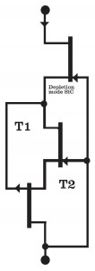
He put a p-channel jfet in place of the resistor (see figure 2).

In this configuration, the channel on-resistance of each jfet acts at the sense resistance for the other’s gate.

When current is flowing from top to bottom, it sees a purely ohmic conduction path consisting of the two channels in series.

Until that is, current reaches the point where one channel voltage drop reaches the Vth of the other jfet – say T2. At this point T2 starts to turn off, which causes the gate voltage of the p-channel jfet T1 to rise, which turns it off. This positive feedback turns both devices off completely in a few µs, and conduction cannot re-start until the power source is removed.

Which fet turns off first depends on the mix of threshold voltages and channel resistances. Fine tuning of these parameters, with due consideration to temperature, allows the trip current to be set – or rather, to set the minimum current that always passes, and the minimum current that never passes.

“At the threshold, the structure quenches, it pinches-off,” said Mauder. “You need very steep resistance after limit. This is an issue for basic structure. We could also use two depletion mosfets. We are investigating if mosfets or jfets are best. The environmental temperature is important.”

Infineon ocb fet

Fig2: Jfet current block, or ‘lambda diode’

As an aside: this structure conducts backwards, but without the over-current blocking characteristic. When conducting forwards with regulated current or voltage, a well-defined negative resistance region can be measured. This negative resistance was once used in RF oscillators, where the pair was called a ‘lambda diode’.

Although this structure could work at hundreds of amps – it just has to have large junctions – there are two reasons it is not viable at hundreds of volts: firstly, the gates would have to withstand the full blocking voltage – close to a show-stopper for devices handling over 20V. Secondly, high-voltage junctions are far larger than low-voltage junctions. “For good conductivity, you have to have low RDSon,” said Mauder. “For the same RDSon, the area of a high-voltage mosfet is proportional to (voltage blocking)2.5 to V2.6.”

Silber at the University of Bremen originally conceived this structure as the low-voltage control element in a high-voltage transistor related to IGBTs.

IGBTs are great for silicon area as for a given blocking voltage they are far smaller than mosfets.

However, for the NEST-DC consortium, IGBTs have a fundamental limitation: heat dissipation.

“An IGBT always has p-n junction, and for silicon this will drop 0.7V. In reality, they hardly ever get below 1V,” said Mauder.

However big its junction is, if the current limiter has an 0.7V drop and is passing 100A, it is going to dissipate 70W. This means it will need a lot of room around it, and will put a significant dent in the efficiency of the system of which it is part.

“For our OCB fet, we want it to be ohmic, to have no 0.7V knee voltage,” said Mauder. So the high-voltage element has to be a jfet or a mosfet, and dissipation can now be arbitrarily low, as long as the fet channel is big enough – which is not such a big problem as fighting the V2.5 issue mentioned above – more of this later.

Infineon ocb fet

Fig3: Cascode allows a low voltage mosfet to switch high voltage via a jfet

Mauder is proposing to use a cascode structure – see figure 3.

Originally proposed as a way to improve the bandwidth of RF amplifiers, cascode switching has really caught on in power circuits since GaN ‘hemt’ and SiC jfet power devices have appeared – both of which are depletion-mode in nature.

With a cascode, a high-voltage depletion-mode GaN or SiC transistor can be turned on and off by a far smaller low-voltage enhancement-mode silicon mosfet.

When the mosfet in Figure 3 is turned off by a control signal that pulls its gate to ground, the source voltage of the high-voltage SiC JFET rises and the JFET turns off because its gate is now negative with respect to its source.

The Si mosfet has to carry the same current as the high-voltage device, but it can be far smaller because the maximum voltage across it is the Vth of the depletion-mode transistor, seldom above 20V.

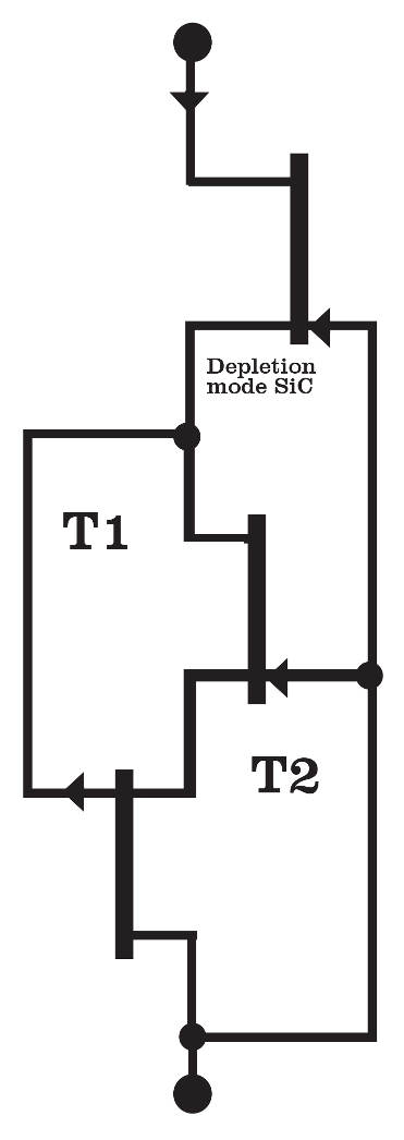
Infineon’s proposed structure replaces the cascoded low-voltage Si mosfet with the double jfet current limit – see figure 4.

Full device current still flows through the jfets but, like the cascode Si mosfet, only have to withstand the Vth of the high-voltage transistor and so can be two small low-voltage jfets.

Infineon ocb fet

Fig4: Over-current blocking fet

The high-voltage transistor still needs a large area, but that is one large junction rather than two – with no gate voltage problems. And, for a given blocking voltage, both SiC and GaN transistors are smaller than their Si cousins, which is why the V^2.5 area issue diminishes. Infineon makes SiC jfets up to 1,700V.

This is a lightning-fast device and, particularly as electronic loads tend to have capacitive inputs, might get tripped-out by switch-on surges.

“There are certain strategies being investigated by partners to do filtering on this basic idea so very short transients do not trip the safety device immediately – for example some RC on the gate [in figure 4]“, said Mauder.

The whole device is a self-contained two-terminal component that does not need an external power supply and has no other inputs through which it might be damaged by external failures – which are reasons Infineon didn’t go the obvious route and combine an existing high-voltage transistor with a sense resistor and a comparator.

“Not needing any external supply for me is big advantage. What happens if the auxiliary supply fails? – Either you get uncontrolled current flow or it disconnects. We are able to do over-current turn-off without need of external current measurement,” said Mauder.

However, if more than two terminals can be accepted, Mauder has another trick up his sleeve.

SiC and GaN transistors are made on expensive processes. Could the high-voltage transistor be a simple silicon mosfet, which would also allow the whole OCB FET to be monolithically integrated?

Infineon popularised the ‘super-junction’ mosfet when it introduced its first CoolMOS branded devices. Super-junction transistors use a structural trick to reduce die area more than is possible with conventional high-voltage mosfets.

A second branch of NEST-DC is a project to further improve super-junction mosfets so they can be used to replace the SiC jfet in figure 4.

“We are investigating a new way for super-junction devices to reduce RDSon x area. State-of-the-art is 6.2Ωmm2 or even more, and we want to considerably reduce this value and chip area,” said Mauder.

Some simulations have already been done and show it is possible. “Now we have to have a closer look via simulation and experimentation. We need to retain ruggedness and avalanche capability. I have good feeling we can do that,” he said.

However, super-junction mosfets are enhancement-mode devices, so an all-silicon version would need an auxiliary supply.

“Since there is no frequent switching needed, this auxiliary supply might be a super-capacitor or something similar which could supply the gate of the high-voltage enhancement MOS over pretty long time – hours or even for days,” said Mauder.

And once an auxiliary supply is accepted, the current limit can become a switch as well as a breaker.

“In most applications, a remote access to such a safety switch is wanted anyway to use it as a conventional switching element. One could use this access to turn-on and turn-off the safety switch via charging or discharging the super-cap auxiliary supply,” said Mauder. “In case of a failure of the remote access, the safety switch still has its stand-alone capability to respond to overcurrent without additional devices or additional supply voltages [if the super-cap is charged].”


Making music with Arduino and the Raspberry Pis

Raspberry Pi B+

Raspberry Pi B+

RS Components is organising a design competition which gives Arduino or Raspberry Pi computer modules a musical flavour.

This is part of the distributor’s sponsorship of the Music Tech Fest London, taking place from 5-7 September at the London Symphony Orchestra’s own venue, the LSO St Lukes.

The challenge will be to complete the project, dubbed hack challenge, in 24 hours. It will then give a showcase performance of each hack challenge on the main festival stage. A live YouTube stream will highlight the results and the winning hackers will be presented with a prize donated by RS.

RS is also sponsoring a collaboration between pro hacker Adam John Williams and solo artist Jason Singh, who uses his voice and samplers to engage people in musical creation.

Guy Magrath, global head of eCommerce at RS Components said: “As a business that has helped engineers to innovate for over 75 years, we are embracing the digital age by supporting futuristic projects and events like Music Tech Fest that bring the application of components to life. For us, the three-day event is the perfect platform to leverage the expertise of engineers and hackers, and bring their knowledge to life by demonstrating the use of components in various ways. We are delighted to be involved with Music Tech Fest and the opportunity it presents in developing new applications of components in music.”


Asenov sells statistical process IP to GloFo

Professor Asen Asenov

Professor Asen Asenov

Gold Standard Simulations (GSS), professor Asen Asenov’s IC production statistical analysis company, has signed a multi-million dollar contract to license its complete TCAD/EDA tool suite to Globalfoundries.

The fully integrated and automated tool chain includes Garand, the GSS ‘atomistic’ TCAD simulator; Mystic, the GSS statistical compact model extractor; and RandomSpice, the GSS statistical circuit simulator.

The GSS tool suite is the world’s only fully integrated tool chain that performs simulation- based design/technology co-optimisation (DTCO) in advanced bulk, FDSOI and FinFET CMOS technologies, including statistical variability and reliability.

“The GSS simulation tools offer significant competitive TCAD advantages that support technology development by providing a seamless flow from Monte Carlo transistor simulation through physical simulation of statistical variability, extraction of accurate statistical compact models, and circuit simulation,” said GloFo’s Francis Benistant. “This integrated tool-chain provides a highly efficient TCAD environment that greatly accelerates technology design and circuit co-optimisation to accelerate technology development.”

“We are delighted to have Globalfoundries as a GSS customer. I believe this relationship will prove to be highly symbiotic and will lead to advances in both Globalfoundries technology offerings and in driving future developments in the GSS tool chain,” said Asenov, who is professor of electrical engineering at Glasgow University as well as CEO of GSS.

“The significance of this is that a small start-up company from Scotland with no venture capital has won a multimillion-dollar deal with the second largest foundry in the world,” added Asenov. “This is in competition with mighty EDA companies like Synopsys.”

Silego CMICs have soft-start power switching

Silego SLG46116VSilego has brought out two more CMICs (configurable mixed-signal ICs) in its GreenPak (GPak) series of tiny, fast to programme, configurable ICs.

The SLG46116V and SLG46117V are the first GPAK devices to enable 1 A P-Channel mosfet soft-start power switching, controlled with a mixed-signal matrix, in a 1.6×2.5×0.55 mm seven-GPIO STQFN package.

The soft-start power switch has fixed slew rate control, and is available with an integrated discharge path (SLG46117V) or without (SLG46116V).

SLG46116V and SLG46117V projects use GPak development hardware and GPak Designer.

“Silego’s latest devices add intelligent power switching functionality to the analogue and digital functions provided by GPAK,” said Silego’s Nathan John.

Four lasers conjure fibre optic out of thin air

Professor Howard Milchberg

Professor Howard Milchberg

Optical fibres made from thin air could transmit data to and from hard-to-reach places.

Regular optical fibres are made from two transparent materials that slow light down by different amounts. The difference in materials lets light reflect along the length of the cable without leaking out – perfect for sending a signal over long distances.

But it’s hard to put fibres in some places, like the upper atmosphere or inside nuclear reactors. And signals sent through open air often degrade because the light spreads out.

Now, Howard Milchberg of the University of Maryland, College Park, and his colleagues have come up with a way to mimic a fibre in the air itself.

The team shone four lasers in a square arrangement, heating air molecules and creating a low-density ring around a denser core of air. Light bounces around the dense core just like in a fibre.

The air fibre lasts for a few milliseconds – more than enough to send a signal. “This is an extremely long time from the vantage point of a laser,” says Milchberg. The results are published in the journal Optica.

So far the team has tested air fibres over a range of 1 metre. These delivered a signal 50 per cent stronger than through air alone over the same distance. Sending signals further gives light more chance to spread, so in theory, a 100-metre air-fibre could deliver a signal 1000 times stronger than sending it through air alone.

The team also transmitted a laser with 100 times more energy than those used to make the fibre. And they were able to receive signals: small flashes of light from the other end were detected. This suggests the fibre could be used for remote sensing, which could include detecting explosives at a distance.

Syndicated content: Jacob Aron, New Scientist

Google offers $1m power inverter challenge

Google little box challenge

Google little box challenge

Google, together with the IEEE, is offering $1m to the person or team who best shrinks the size of power inverters, in something called the ‘Little box challenge‘.

“We’re looking for someone to build a kW-scale inverter with a power density greater than 50W/inch3,” said the firm, which is suggesting wide bandgap semiconductors (GaN or SiC, for example) could be part of the answer.

As such, it has teamed up with SiC and GaN vendors: Cree, Efficient Power Conversion, GaN Systems, Monolithic Semiconductor, NXP, Rohn, Transphorm, and United Silicon Carbide.

A test facility will be set up in the US to evaluate potential winners.

The competition is open worldwide to anyone, individuals, teams, companies, and academics. For the latter, grants of around $25,000 are available from Google.

Timetable:

  • Registration by 30 Sep 2014
  • Submit approach by 22 Jul 2015
  • Final date for testing 21 Oct 2015.
  • Winner announced Jan 2016

Google is not requiring any intellectual property or licenses be granted, except a non-exclusive license to be used only for the purpose of testing the inverter and publicising the prize.

News 2014-07-22 08:45:00

 st-rad-hardSTMicroelectronics has added to its range of Defense Logistics Agency-qualified JANSR bipolar transistors with additional up-screening.

Designed for aerospace systems, including satellites, as well as nuclear physics and medical applications, the radiation hardened transistors were announced at the recent Nuclear and Space Radiation Effects Conference (NSREC) in Paris.

Called JANSR+, the high-dose-rate bipolar transistors have an additional 100krad low-dose-rate (100 mrad/s) test performed on each wafer.

ST also said it will complete its JANSR+ offer with test data from very-low-dose-rate (10 mrad/s) tests, demonstrating the robustness to radiation effect of its technology.

“ST has been providing rad-hard bipolar transistors to the European aerospace industry for over 35 years and our products have accumulated hundreds of millions of flying hours,” said Mario Aleo, group v-p and general manager, power transistor division, STMicroelectronics.

All parts are housed in advanced hermetic UB packages and are available in sample and volume quantities.

Good Q2 for ARM

ARMV8-AARM had Q2 revenues of $309m, up 17% year-on-year for a profit of $160m.

Forty-one new licences were signed in Q2, six of which were by first time licensees.

“The 41 processor licences signed in Q2 were driven by demand for ARM technology in smart mobile devices, consumer electronics and embedded computing chips for the internet-of-things (IoT), and include further licences for ARMv8-A and Mali processor technology,” said Simon Segars, “this bodes well for growth in ARM’s medium and long term royalty revenues

Seven new ARMv8-A licences were signed – taking the total to 50 licenses with 28 partners, eight of which are in China.

It was a record quarter for new Mali licences. Eight Mali multimedia processor licences were signed, including the first licences for video and display processors

Processor licensing revenue was up 42% year-on-year, and processor royalty revenue was up 2% year-on-year.

There was 11% growth year-on-year in overall unit shipments, to 2.7 billion ICs.

During the quarter, ARM delivered the Juno development platform to support the development of the next generation of Android L devices on the ARM V8-A architecture.

Three semiconductor vendors debuted ARM-based server solutions

“Market data indicates improving semiconductor industry conditions, leading to the expectation of an acceleration in royalty revenue growth in H2 2014.”


Current-voltage monitor has 16-bit precision

Digital-Power-MonitorIntersil has introduced a family of digital power monitors capable of supporting a wide common mode input voltage range of 0 to 60V.

The ISL2802x range of devices have a 16-bit native resolution sigma-delta ADC (gain error = +/- 0.05% Typ.) for measurement precision and are available as bi-directional, high-side and low-side digital current sense and voltage monitors with a serial interface.

The devices can be used to replace op amps and current sense amplifiers traditionally used for voltage and current measurement.

The three devices in the family are:

  • The ISL28023 PMBus compatible digital power monitor that integrates the analog comparators, a voltage regulator, a DAC and a low voltage auxiliary channel in a single chip.
  • The ISL28025 is a high precision digital power monitor with integrated analog comparators and an integrated voltage regulator.
  • The ISL28022 is a highly efficient digital power monitor ideal for cost constrained applications.

Operating temperature range is from -40ºC to 125ºC.

“We’ve taken the best of our current sense amplifier technology and augmented it with digital power monitoring to deliver a robust and highly accurate, but simple to use family of digital power monitors,” said Philip Chesley, vice president of Precision Products for Intersil.