Japan creates a super OLED company

Sony and Panasonic are to combine their R&D for organic light-emitting diode (OLED) displays in a new company, which will effectively be owned by the government-backed public-private partnership agency, the Innovation Network Corporation of Japan (INCJ) and Japan Display Inc. (JDI).

The new company to be called JOLED will launch in 2015. INCJ and JDI will respectively hold 75% and 15% of the voting rights in JOLED, and Sony and Panasonic will each hold 5%.

INCJ and JDI plan to make additional investments to fund a pilot manufacturing plant when the OLED technology is ready for commercialisation.

The OLED display technologies Sony and Panasonic bring to the venture including use of printing technology, transparent amorphous oxide semiconductors and flexible display technology.

In addition, JOLED plans to take advantage of JDI’s wide-ranging portfolio of display technologies. JOLED’s aim is to become the leader in the global OLED display market.

JOLED plans to focus primarily on development of medium-size OLED displays for use in tablets, mobile PCs, and signage.

INCJ was established in 2009 as a public-private partnership to support technology ventures.

It has the capacity to invest up to ¥2 trillion (approx $20bn), and to date, INCJ has invested approximately ¥750 billion in a total of 71 projects.

Earlier this year, the INCJ stepped in to form JDI when Sony, Toshiba and Hitachi were hit by a collapse in TV sales partly caused by the success of Samsung.


richard wilson

Sheffield University spray paints solar cells

The two spray heads. (Picture by Alex Barrows)

The two spray heads. (Picture by Alex Barrows)

A team of scientists at the University of Sheffield are the first to fabricate perovskite solar cells using a spray-painting process – a discovery that could help cut the cost of solar electricity.

Experts from the university’s Department of Physics and Astronomy and Department of Chemical and Biological Engineering have previously used the spray-painting method to produce solar cells using organic semiconductors – but using perovskite is a major step forward.

Efficient organometal halide perovskite-based photovoltaics were first demonstrated in 2012. They are now a very promising new material for solar cells as they combine high efficiency with low materials costs.

The spray-painting process wastes very little of the perovskite material and can be scaled to high volume manufacturing – similar to applying paint to cars and graphic printing.

Lead researcher professor David Lidzey says: “Perovskite-based photovoltaics combine the high performance of mature solar cell technologies with the low embedded energy costs of production of organic photovoltaics.”

While most solar cells are manufactured using energy intensive materials like silicon, perovskites, by comparison, requires much less energy to make. By spray-painting the perovskite layer in air the team hopes the overall energy used to make a solar cell can be reduced further.

Lidzey adds: “The best certified efficiencies from organic solar cells are around 10%. Perovskite cells now have efficiencies of up to 19%. This is not so far behind that of silicon at 25% – the material that dominates the world-wide solar market.”

“The perovskite devices we have created still use similar structures to organic cells. What we have done is replace the key light absorbing layer – the organic layer – with a spray-painted perovskite,” says Lidzey. “Using a perovskite absorber instead of an organic absorber gives a significant boost in terms of efficiency.”

The Sheffield team found that by spray-painting the perovskite they could make prototype solar cells with efficiency of up to 11%.

“This study advances existing work where the perovskite layer has been deposited from solution using laboratory scale techniques. It’s a significant step towards efficient, low-cost solar cell devices made using high volume roll-to-roll processing methods,” Says Lidzey.

david manners

DC-DC converter in a BGA has 2kV isolation

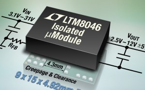
LinearTechLinear Technology has introduced a 2.5W output DC/DC converter with 2kVAC galvanic isolation in a 9x15x4.92mm ball grid array (BGA) package.

The isolated transformer, control circuitry, power switches, and a modest amount of input and output capacitance are encased in the BGA package.

A minimum creepage distance of 4.3mm on the package exterior supports operation at a working voltage up to 400VRMS in a pollution degree 2 environment. This classification is important as it affects parameters required to ensure safe operation of the product.

Pollution degree 2 refers to an environment where normally only non-conductive pollution or temporary condensation may occur, such as in offices, laboratories and test stations.

The isolated µModule converter operates from an input voltage of 3.1V to 31V, delivering a regulated output voltage on the secondary side, adjustable from 1.8V to 12V with ±5% accuracy over temperature.

Even if input voltage is above, below or equal to the desired output voltage, says the supplier, the internal flyback architecture enables the LTM8046 to maintain output voltage regulation.

It will deliver the full 2.5W output power at ambient temperatures up to 100°C with no forced airflow.


richard wilson

300kW SiC half-bridge offers 99% efficiency

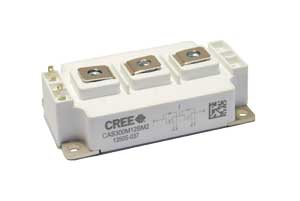
Cree SiC AS300M12BM2Silicon carbide is a route 99% efficiency in induction heating drivers, claimed Cree as it introduced a 300A, 1.2kV half-bridge module.

Bolting straight into a industry-standard 62mm footprint, it includes two 5mΩ SiC mosfets and two SiC free-wheeling Schottky diodes, that drop 1.7V at 300A.

“The power module is pin-compatible to 62mm half-bridge modules, including IGBT modules rated at 450A or more, allowing designers to evaluate the module’s capabilities,” said Cree.

Dubbed CAS300M12BM2, price is $451 each for 1,000-unit quantities.

Other applications foreseen are: solar Inverters and variable-frequency motor drives.

A matched driver board (CGD15HB62P) is also available, which will operate the half-bridge on DC bus voltages up to 900V at up to 32kHz – or 64KHz with some component swaps.

It is completely isolated and includes everything required to interface microcontroller PWM waveforms to the half-bridge. It does need a 15V power rail on the microcontroller side.

A gate driver reference design is also available.

steve bush

Microchip makes record profits in Q1

MicrochipMicrochip Technology has reported increased sales for the three months ended June 30.

Consolidated GAAP net sales for the first quarter of fiscal 2015 were a record $528.9m, up 7.2% sequentially and up 14.3% from the same quarter last year.

Net income for the first quarter of fiscal 2015 was $89.9m. This was lower than the preceding quarter, but 14.4% up on the first quarter last year.

Non-GAAP net sales for the first quarter were a record $531.3m and non-GAAP net income for the first quarter was $151.6m.

According to Steve Sanghi, Microchip president and CEO: “We are making excellent progress towards our long term goal of 35% non-GAAP operating profit.”

Sanghi said he sees ”seasonally normal business environment with strengths in many of our end markets like industrial, automotive, housing, consumer electronics and personal computing”.

“We are seeing exceptional strength in some of our new products and technologies which are growing revenue at double digit percentages sequentially. Our inventory of 108 days is below our targeted level of 115 and is expected to go lower this quarter. We are ramping all of our factories, but are limited by equipment lead times. We have increased our planned capital expenditures for fiscal year 2015 to $175 million.”

The firm’s microcontroller revenue grew 5.3% sequentially and was up 14.5% on Q1 2014. According to Ganesh Moorthy, Chief Operating Officer: ”All three microcontroller product lines, 8-bit, 16-bit and 32-bit experienced sequential revenue growth”.


richard wilson

Murata improves accuracy of crystals

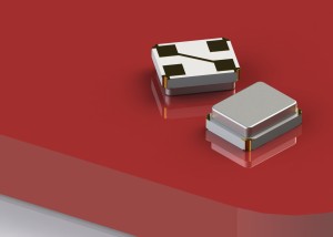
 murataMurata has improved frequency tolerance and temperature characteristics of its crystal devices.

The XRCGB-F-P series has a frequency tolerance of +/- 20 ppm (at +25 deg C), and frequency shift by temperature of +/- 20ppm max. (-30 to + 85 deg C).

Compared to previous crystal units that had a combined tolerance of +/- 70ppm, these +/- 40ppm units represent close to a 43% improvement in total tolerance.

In addition to the tolerance improvements the XRCGB-F-P series are constructed in the popular 2016 package.


richard wilson

Intel Baytrail in COM Express at RDS

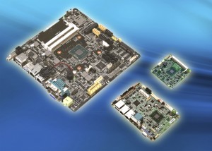
 RDSReview Display Systems (RDS) is offering three embedded boards from AAEON based on Intel’s latest Baytrail range of CPU platforms.

For handheld and space conscious applications, where users have configured their own base board, using the compact COM Express Type 6 format CPU module, the COM-BT, is available in single, dual and quad core versions, based on the Intel Atom E3815 (single), E3827 (dual) and E3845 (quad) processors.

It will support up to 4Gbyte DDR3L 1066/1333MHz SODIMM, two SATA 3Gbit/s I/O ports and an option 4GB eMMC port.

The board supports two simultaneous display outputs: VGA, DVI, HDMI, DP and eDP. There is also a high-definition audio interface and support for Intel Gigabit Ethernet.

The GENE-BT05 is a 3.5-inch, feature rich industrial sub-compact motherboard and features Intel Celeron N2930/ N2807 processors, with 204 pin SODIMM DDR3L, maximum 8Gbyte of system memory, and twin Gigabit Ethernet.

It supports CRT/LCD, HDMI/LCD simultaneous or dual view displays. A four-, five- or eight-wire resistive touch screen is available as an option.

The largest of the three formats is the EMB-BT1 thin Mini-ITX embedded motherboard is based on Intel Atom E3845/E3825 processors, delivering 1.91GHz and 1.33GHz respectively. The dual display board supports VGA, HDMI and LVDS and has SATA 6Gbit/s x 2 and SATA 3Gbit/s x 2 I/O ports.


richard wilson

Mobile to be biggest consumer of DRAM, says IC Insights

This year, for the first time ever, mobile applications will use more DRAM than computers, reports IC Insights.

“In 2014 mobile systems are forecast to become the largest application for DRAM bit volume, surpassing the desktop/notebook segment, which has long been the essential driver for DRAM bit consumption,” says IC Insights.

The slowdown in PC shipments has considerably affected where DRAM bit volume is being consumed.

The desktop/notebook computer segment represented less than half of total DRAM bit volume for the first time in 2012 and its share is forecast to fall to 31% in 2014 — half its market share from 2010.

DRAM bit growth, which averaged 83% annually between 1995 and 1999, has been running at 36% annually since 2010.

david manners

Vishay turns to nitride for high-power chip resistors

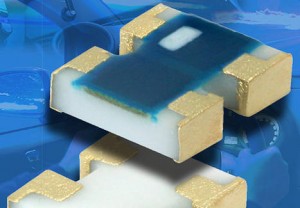
Vishay PCAN AlN resistorVishay is using aluminium nitride substrates to achive 2W and 6W power handling in 1206 and 2512 chip resistors, respectively.

Called PCAN, they also have enlarged backside terminations to reduce thermal resistance between resistive element and PCB solder joint.

“The devices provide four times the power handling capability of commercial chip resistors,” said the firm, which is aiming them at power supplies for industrial, telecommunications, test, measurement, medical, military and aerospace.

They have ±25ppm/°C and 0.1ppm/V coefficients, and laser-trimmed tolerances down to ±0.1% over -55°C to 150°C.

Values between 30Ω and 175Ω are available with 75 to 200V ratings.

Flame-resistant in accordance with UL 94 V-0.

Pb-free wrap-around terminations are standard, with Pb-inclusive, wire-bondable gold, and epoxy-bondable (glueable) gold options.

steve bush

Wearable wireless goes Bluetooth Smart

IHS Wireless_Semiconductor_ShipmentsShipments this year for wireless semiconductors in health and fitness will reach a projected 61.2 million units, up 11% from 55 million in 2013, and will increase to 95.78 million units in 2018, says IHS, while shipments  of consumer health and fitness devices with integrated wireless connectivity will grow to an estimated 75.7 million units in 2018, up from 23.0 million units in 2011.

Bluetooth Smart is the main medium for wireless connectivity in this market.

Wireless connectivity in sports and fitness applications is often used to provide a link to remote sensors when wired connectivity is too cumbersome, like linking heart-rate chest straps to wrist-worn heart-rate monitors, or linking wheel-speed sensors to cycling computers.

Another use is for data uploading, with wireless connectivity employed to upload fitness and performance data to PCs, smartphones, tablets or online communities for analysis and sharing.

Bluetooth Smart I, says IHS,is  the only major low-power wireless technology able to communicate with all the chief mobile platforms, including Apple iOs, Google Android, Microsoft Windows 8 and the BlackBerry operating system, says IHS.

Moreover, the dongle-free connectivity of Bluetooth Smart gives it an edge..

A wireless technology specifically designed for the health and fitness market and popular with heart-rate monitors, ANT/ANT+, is a low-power technology that, however, does not enjoy the same broad support in mobile platforms.

A PC or dongle is also required for ANT/ANT+, unlike Bluetooth Smart. Still, ANT/ANT+ enjoys a significant market share and seems to have a defensible position, especially in products designed for serious fitness enthusiasts and in cycling electronics.

A big driver of growth in health and fitness devices is the desire among consumers to track and analyse personal data, in pursuit of what is known as “the quantified self,” says IHS. Consumers can then share such data via social media and online communities, often via apps like RunKeeper of Runtastic.

Other drivers for the market include the increased use of wearable devices; decreasing component costs; an ageing demographic concerned about preserving health; and the rising use of remote healthcare systems.

david manners