Intel buys into Spreadtrum and RDA to push mobile x86 into China

Intel CEO Brian Krzanich

Intel CEO Brian Krzanich

Intel has bought a 20% share in the China state-owned company, Tsinghua Unigroup, which owns mobile chip developers Spreadtrum and RDA. The two chip companies will now make x86-based mobile ICs.

With China’s mobile IC specialist RockChip already co-developing chips with Intel, Intel has ensured that three of China’s major mobile chip-makers, which used to make ARM-based chips, will now make x86-based chips.

In December 2013, Unigroup bought Spreadtrum for $1.75 billion and in July this year Unigroup bought RDA for $907 million.

“This collaboration and investment will also enhance our ability to support a wider range of mobile customers in China and the rest of the world,” said an Intel spokesperson, “we will be able to deliver a broader portfolio of Intel architecture and communications technology solutions.”

“China is now the largest consumption market for smartphones and has the largest number of Internet users in the world,” said Brian Krzanich, Intel CEO, “these agreements with Tsinghua Unigroup underscore Intel’s 29-year-long history of investing in and working in China. This partnership will also enhance our ability to support a wider range of mobile customers in China and the rest of the world by more quickly delivering a broader portfolio of Intel architecture and communications technology solutions.”

Zhao Weiguo, chairman and president of Tsinghua Unigroup, says, “It has become a national priority of China to grow its semiconductor industry. The strategic collaboration between Tsinghua Unigroup and Intel ranges from design and development to marketing and equity investments, which demonstrate Intel’s confidence in the Chinese market and strong commitment to Chinese semiconductor industry, which will accelerate the technology development and further strengthen the competitiveness and market position of Chinese semiconductor companies.”

Spreadtrum will mske x86-based mobile SoCs coming on the market in H2 2015 to be sold both by Intel and Spreadtrum.

“The adoption of Intel’s architecture technology will enable us to accelerate the development of mobile SoCs that expand the breadth of our portfolio, benefiting handset makers addressing both China and the global market,” said Leo Li, chairman and CEO of Spreadtrum, in a statement. “We are pleased to embark on collaboration with Intel around these new product offerings.”

david manners

≤28nm processes account for 71% of all foundry revenues, says IC Insights

IC Insights - Foundry Revenue per logic waferTSMC has 84% of the total ≤28nm pure-play foundry market this year with $10.3bn in ≤28nm sales, says IC Insights.

Overall, ≤28nm foundry revenues will grow 72% in 2014.

Of the big four pure-play foundries (TSMC, GlobalFoundries, UMC, and SMIC), TSMC is the only one that is expected to have a higher revenue-per-wafer figure in 2014 than in 2010.

Of the big four foundries, TSMC is forecast to have the highest revenue per wafer in 2014 at $1,328, 27% higher than GlobalFoundries.

In contrast, UMC’s revenue per wafer in 2014 is expected to be only $770, 42% less than TSMC’s revenue per wafer.

Although the average revenue per wafer of the big four foundries is forecast to be $1,145 in 2014, the actual revenue per wafer is highly dependent upon feature size.

There is more than a 14-times difference between the 0.5µ 200mm revenue per wafer ($430) and the 28nm 300mm revenue per wafer ($5,850).

Even when normalising the figures by using the revenue per square inch, the difference is dramatic ($51.77 for the 28nm technology versus $8.56 for the 0.5µ technology).

Although TSMC has a very large percentage of its sales targeting ≤45nm production, its 2014 revenue per wafer is still forecast to be up only 14% when compared to 2009.

IC Insights believes that the entrance of GlobalFoundries and Samsung into the high-end foundry market over the past few years has put pressure on TSMC to keep its prices for leading-edge products competitive.

Although there will probably be only five foundries able to offer high-volume leading-edge foundry production over the next five years – TSMC, GlobalFoundries, UMC, Samsung, and Intel – these companies are likely to be fierce competitors and pricing will likely be under pressure as a result.

Before GlobalFoundries entered the foundry market, TSMC was by far the technology leader among the major pure-play foundries.

In 2014, 60% of TSMC’s revenue is expected to be from ≤45nm processing.  As expected, with GlobalFoundries’ fabs having a large portion of their capacity dedicated to producing AMD’s MPUs over the past few years, its processing technology is skewed toward leading-edge feature sizes.

In 2014, 57% of GlobalFoundries’ sales are forecast to be from ≤45nm production.

Although GlobalFoundries is expected to have a similar share of its sales dedicated to ≤45nm technology as TSMC in 2014, TSMC is forecast to have almost six times the dollar volume sales at ≤45nm as compared to GlobalFoundries this year ($14.8bn for TSMC and $2.5bn for GlobalFoundries).

In contrast, only 15% of SMIC’s 2014 sales are expected to come from devices having ≤45nm feature sizes, which is the primary reason why its revenue per wafer is so low as compared to TSMC and GlobalFoundries.

The vast majority of the increase in pure-play foundry sales in 2014 is forecast to be due to ≤28nm feature size device sales.

Although it is expected to represent 71% of total pure-play foundry sales in 2014, the >28nm pure-play IC foundry market is forecast to increase only 4% this year.

In contrast, the 2014 leading-edge ≤28nm pure-play foundry market is expected to be about $5.1bn, a 72% increase in size as compared to 2013.

Not only is the vast majority of pure-play foundry growth coming from leading-edge production, most of the profits that will be realized come from the finer feature sizes as well.

david manners

New energy efficiency rules will change motor control design

 ADSP-CM408F_ez-kitMotor control is becoming the power industry’s fastest changing technology area. The reason for this is the requirement to improve energy efficiency from the millions of motors which are used in our homes, factories and cars.

New developments in motor controller design, current sensing and control algorithms will be needed if new and more stringent efficiency targets are to be achieved.

The main design elements of motor control can be broken down into four parameters – communications interface, EMC robustness, circuit isolation and energy efficiency.

It is in the area of energy efficiency where the biggest changes are likely to take place in the next few years.

According to Anders Fredriksen from Analog Devices, there is a big push to put more importance on energy efficiency in motor design, and this will increase over the next few years as new efficiency standards are introduced.

“Standardisation has been going on for decades but by 2017 extensions to energy efficiency guidelines being applied to motors down to 1W will have the biggest impact for manufacturers,” said Fredriksen.

But Frederiksen believes further advances in motor control design are still needed to meet the requirements of the new energy efficiency standards.

“There may be a need to change motor control architectures, we won’t achieve all the new efficiency standards without this,” said Fredriksen.

This will apply to the industrial motors as well as those in household appliances and cars.

This drive to increase energy efficiency needs to be applied at the component level. This means adding processor power to motor controllers to run the optimisation algorithms. It also requires increased accuracy when current sensing.

“For example, the use of isolated sigma-delta conversion for higher accuracy,” said Fredriksen.

ADI offers a high accuracy isolated sigma-delta converter for dc and ac current and voltage measurement.

The AD7403 achieves 81dBmin signal-to-noise and distortion ratio (SINAD, at 78ksample/s over -40 to 125°C). Higher SINAD enables more accurate current and voltage measurement which improves the performance of motor drives by reducing torque ripple on the motor shaft.

It has a second-order, sigma-delta modulator that converts an analogue input signal into a single-bit data stream with on-chip digital isolation (1,250Vpeak) through on-chip transformers.

Operation is from 5V at the measurement end and it accepts a differential input signal of ±250mV (±320mV full-scale). The analogue input is continuously sampled and converted to a ones-density bit stream with a data rate of up to 20MHz. The original information can be reconstructed with appropriate digital filtering to achieve 88dB signal to noise at 78.1ksample/s.

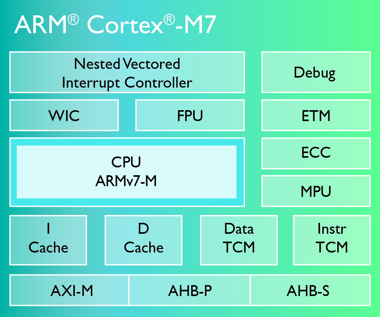
For data processing, microcontrollers are moving to higher performance cores such as the ARM Cortex-M4, which has DSP extensions.

“There has been a lot of work going on around algorithm development for motor control, the increase in processing capability which cores like the Cortex-M4 provide has brought these advanced algorithms into play,” said Fredriksen.

For example, minimising torque ripple on the motor shaft can improve productivity.

Analog Devices has combined an ARM Cortex-M4 processor and a model-based design platform to address the needs of closed loop motor control.

The floating-point Cortex-M4 processor core runs at 240MHz and ADI has also integrated a dual 16-bit A/D converter with up to 14 bits of accuracy and 380ns conversion speed.

ADI’s previous motor controller platform was based on its own ADSP-BF506A Blackfin processor, but it has realised that the Cortex-M4 was quickly becoming the de facto standard architecture for accurate control systems.

Fredriksen also believes that model-based design tools such as Simulink from the MathWorks are now becoming important in the development of control systems for motors and PV arrays.

Two years ago ADI demonstrated its first motor control system design platform, based on a Blackfin processor, using the MathWorks Matlab computing language for algorithm development.

It also implemented the Simulink design environment for the deployment of control algorithms to optimise the efficiency of permanent magnet synchronous and ac induction motors.

The intention was to allow designers to model their system in Matlab/Simulink, generate the C code, and deploy with Analog Devices’ Visual DSP++ Design Environment with bandwidth remaining for application code.

Fredricksen believes that the use of model-based designs can improve the drive efficiency of sensorless and sensored motor control algorithms.

ADI has worked with the MathWorks to apply the Simulink model-based design tool and code generator to its motor control platform. It uses the MathWorks’ ARM Cortex-M optimised Embedded Coder and tool suites to support the complete design cycle from simulation to product-ready code implementation in an embedded platform.

Simulink generates optimised C code which runs on the Cortex-M4 based platform. The company has also increased the on-chip memory to 384kbyte of SRAM to hold the C code generated by the tool.

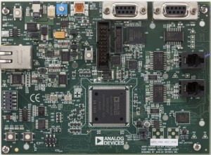
The ADSP-CM40x has control loop specific hardware accelerators, a full sinc filter implementation to interface directly to isolated sigma-delta modulators which are used in shunt-based current sensing system architectures. Typically, the sinc filter would have been implemented in an FPGA.

There is also a DSP accelerator providing harmonic analysis typically used in PV array control loop design.

It is also capable of scalable and dynamically adjustable PWM.

There is a development and evaluation board, CM40xEZBoard, supported by standard control algorithms.


richard wilson

Freescale plans first Cortex-M7 based Kinetis MCUs

Freescale-kinetis Freescale Semiconductor is bidding to be first to market with chips based on ARM’s latest processor core and it plans Kinetis family microcontrollers with the ARM Cortex-M7 core.

The Cortex-M7 processor has been designed for higher performance and doubles the performance of previous Cortex-M4 processors. Target applications are likely to be high end motor control, video and power conversion.

“The new ARM Cortex-M7 processor delivers truly exceptional performance and energy efficiency,” said Denis Cabrol, head of global marketing and business development for Freescale’s MCU group.

Freescale will maintain software and hardware compatibility across its six Kinetis MCU families.

Noel Hurley, general manager, CPU group, ARM commented:

“Freescale has long been a trusted ARM partner and key early adopter of our newest technologies. We value the insight that Freescale and their customers have given us in determining the functionality for the Cortex-M7 processor.”


richard wilson

Qualcomm extends domination

Sravan Kundojjala

Sravan Kundojjala

Qualcomm’s baseband processor market share is at a record 68% with MediaTek No. 2 on 15%and Spreadtrum on 5% at No. 3, says Strategy Analytics.

The global cellular baseband processor market grew 17% year-on-year to reach $5.2 billion in Q2 2014.

Qualcomm, MediaTek, Spreadtrum, Marvell and Intel grabbed the top-five baseband revenue share spots in Q2 2014. Qualcomm continued its baseband market dominance with 68 % revenue share, followed by MediaTek with 15 % revenue share and Spreadtrum with 5 percent revenue share.

Sravan Kundojjala, Senior Analyst states, “Despite increased LTE baseband competition, Qualcomm managed to increase its baseband revenue share to an all-time-high of 68 % in Q2 2014. Qualcomm’s LTE Gobi slim modems and LTE Snapdragon applications processors all gained strong traction in Q2 2014 and featured in multiple flagship smartphones. Strategy Analytics calculates that LTE basebands accounted for over 45 % of Qualcomm’s total baseband shipments in Q2 2014. Strategy Analytics believes that still further LTE gains in the next few quarters provide further scope for market share gains.”

According to Stuart Robinson, Director of the Strategy Analytics Handset Component Technologies service, “In Q2 2014, MediaTek capitalised on its baseband-integrated applications processor momentum and solidified its number two position in the baseband market. Strategy Analytics estimates LTE basebands accounted for less than 1 percent of MediaTek’s total baseband shipments in Q2 2014. However, Strategy Analytics believes that MediaTek has the potential to emerge as the number two LTE baseband player in the second half of 2014, thanks to increased traction in China.”

Christopher Taylor, Director of the Strategy Analytics RF and Wireless Component service details, “Spreadtrum maintained its number three baseband revenue share position in Q2 2014, after overtaking Intel in Q1 2014. Strategy Analytics estimates that Spreadtrum’s W-CDMA baseband shipments registered 170 percent year-on-year growth in Q2 2014. Spreadtrum is well-positioned to grab W-CDMA market share dropped by Broadcom as it leaves the market.”

In the 2Q14 smartphone apps processor market, Qualcomm remains the company to beat in mobile processors with investments in CPU, GPU, DSP, RF, location and connectivity technologies well matched to current market trends

The chasing pack are now in a better position to compete as they are now shipping the key competitive products: namely LTE and baseband-integrated-Apps processors.

The global smartphone applications processor (AP) market grew 22 percent year-on-year growth to reach $5.2 billion in Q2 2014.

Based on Strategy Analytics estimates, Qualcomm, Apple, MediaTek, Spreadtrum and Samsung captured the top-five smartphone AP spots in Q2 2014. Qualcomm topped the smartphone AP market with 58 percent revenue share, followed by Apple with 14 percent revenue share and MediaTek with 13 percent revenue share.

According to Sravan Kundojjala, Senior Analyst, “Qualcomm continues to widen the lead and captured a record 58 percent revenue share in the smartphone AP market in Q2 2014, thanks to its strong momentum in LTE smartphones. Strategy Analytics believes that the multi price-tier Snapdragon processor portfolio continues to serve Qualcomm well.”

Stuart Robinson, Director of the Strategy Analytics Handset Component Technologies service details, “Strategy Analytics estimates that stand-alone AP unit share dropped to 21 percent in Q2 2014 compared to 28 percent in Q2 2013 and this can be attributed to increased shipments of low-to-mid range smartphones, which often feature baseband-integrated APs. Stand-alone AP vendors HiSilicon and Samsung are also now shipping baseband-integrated APs in volume to address mid-range smartphones.”

In the 2Q14 tablet apps market, Intel rose to the No.2 position in tablet APs

The non-Apple tablet AP market leadership position continues to change hands. Previously six companies have held the non-iPad tablet AP leadership position, which continues to be a challenging one to sustain due to the relative ease with which tablet OEMs can switch AP vendors.

The global tablet applications processor (AP) market registered a solid 23 percent year-on-year growth to reach $945 million in Q2 2014.

Apple, Intel, Qualcomm, MediaTek and Samsung captured the top-five tablet AP revenue share spots in Q2 2014. Apple maintained its tablet AP revenue share lead with 26 percent revenue share, followed by Intel with 19 percent revenue share and Qualcomm with 17 percent revenue share.

According to Sravan Kundojjala, Senior Analyst, “The non-Apple tablet AP market leadership position continues to change hands and during Q2 2014 it was Intel’s turn. Strategy Analytics notes that previously six companies held the non-iPad tablet AP leadership position, which continues to be a challenging one to sustain. Strategy Analytics believes that Intel is a on a good trajectory to achieve its 40 million tablet AP shipment goal in 2014.”

Stuart Robinson, Director of the Strategy Analytics Handset Component Technologies service adds, “During Q2 2014, HiSilicon, Marvell, MediaTek, NVIDIA and Qualcomm all registered significant shipment growth in the tablet AP market. Strategy Analytics believes that NVIDIA is well-positioned to grab high-profile tablet design-wins with its 64-bit Tegra K1 chip in the second half of 2014.”

david manners

Global Unichip expands interconnect IP

Global Unichip, TSMC’s design arm, has rolled out an expanded interconnect low power IP portfolio for ASICs targeting solid state drive (SSD) applications. The expansion covers ultra low power PCIe 3/4 PHY, DDR3/4, LPDDR3/4 CTRL/PHY and ONFi4.0 IO/PHY.

IP based on the 28HPM/HPC processes in the expanded portfolio are available now, while 16nm macros will be available in Q4 of this year. The first tape out targeting TSMC’S 16FF+ process is expected in October.

The company’s 16nm DDR4 PHY, taped out in November 2013, was the industry’s first.

The company is now expecting to tape out the industry’s first Application Processor platform IP to TSMC’s 16FF+ process at the start of 2015.

Among all NAND applications, SSD is the fastest growing with the Data Center and Enterprise segments showing the greatest potential. GUC addresses that with a complete low power IP portfolio for SSD controllers, including NAND I/O (ONFI, Toggle), DDR I/F (DDR3/4, LPDDR3/4) and Serdes I/F (PCIe-3/4, SATA3/SAS3).

“We have both a low power IP portfolio and an advanced technology roadmap to drive ASIC development for SSD markets to the next level of innovation,” says C. J. Liang, SVP of R&D at GUC.

GUC’s in-house IP portfolio includes DDR, high-speed networking interfaces, high -speed interface SerDes, data converters, hardened ARM cores, and multimedia IP. GUC’s IP ecosystem provides the flexibility to work with IP from GUC, TSMC and other vendors, creating the widest range of design options.

david manners

TSMC makes 16nm finfet ARM v8 processor for HiSilicon

TSMC President and Co-Chief Executive Officer Dr. Mark Liu

TSMC President and Co-Chief Executive Officer Dr. Mark Liu

TSMC says its collaboration with HiSilicon Technologies has produced the foundry segment’s first fully functional ARM-based networking processor with FinFET technology.

TSMC says its 16FinFET process has twice the gate density of TSMC’s 28HPM process, and operates more than 40% faster at the same total power, or reduces total power over 60% at the same speed.

“Our FinFET R&D goes back over a decade” says TSMC Co-CEO, Dr. Mark Liu.

TSMC’s 16FinFET has entered risk production with excellent yields, says the company, after completing reliability qualifications in November 2013.

Built on TSMC’s 16FinFET process, HiSilicon’s processor enables a significant leap in performance and power optimisation supporting high-end networking applications. By leveraging TSMC’s  heterogeneous CoWoS (Chip-on-Wafer-on-Substrate) 3D IC packaging process, HiSilicon integrates its 16-nanometer logic chips with a 28-nanometer I/O chip.

“This networking processor’s performance increases by three fold compared with its previous generation,” says HiSilicon President Teresa He, “it can support virtualisation, SDN and NFV applications for next-generation base stations,routers and other networking equipment.”


david manners

XMOS adds industrial comms development kit

xMOS development boardXmos has announced development boards for its fast and novel xCore-XA microcontroller, that includes an ARM Cortex-M3 alongside its unconventional low-latency 32bit multi-core processor architecture – invented to provide fast deterministic interfacing without interrupts.

The first products aimed at flexible industrial ‘field bus’ communication.

“There are a plethora of field bus standards. A lot are emerging, and this is where the flexibility of software-defined interfacing is really useful,” Xmos product manager Peter Tasker told Electronics Weekly.

This is not the first time Xmos has tacked field bus with a development kit – there was one early in 2013 (IS-BUS sliceCARD), but this is the first to include the Cortex-M3 extension the firm announced this time last year.

It bought the Cortex-M3 in from Energy Micro (even as Energy was acquired by Silicon Labs), along with a handful of Energy’s famously low-power peripherals – including UART, GPIO and USB.

While incorporating hard peripherals went against the grain at Xmos, it gave the firm a chip that could sleep at under 1µA, clip along at 50Mips for 10mA on the ARM core, then fly instantaneously to 500Mips by engaging the proprietary xCores – all for 50mA.

“The ARM can do the easy stuff and the heavy-lifting is done by the xCores,” said Tasker.

XMOS xCore-XAFor industrial use, xCores can run the lower levels of Ethernet and CAN stacks, for example, while the Cortex-M3 handles the upper layers. Libraries are available to aid communication between the dissimilar cores, and there are stacks for CAN and Ethernet on the way.

“Most field busses are built on Ethernet and CAN. We don’t intend to develop loads of stacks. We will have some core stuff like Ethernet and CAN, and we might partner with third-party industrial stack providers to offer their products on our silicon,” said Tasker.

And if a customer wants to develop custom lower stack levels for a different interface?

According to Tasker: “It is pretty easy to implement the low level on xCores – you don’t have to write interrupt service routings. I wrote a DMX 512 [LED lighting] controller in a few hours.”

Aren’t there already plenty of microcontrollers around with Ethernet and CAN interfaces?

Tasker questions their reliability and determinism.

“When CAN is a hard peripheral, the peripheral does the CRC [cyclic redundancy check] and passes only the packet on to the processor. In a bridge, we want to preserve CRC from end to end, all the way from CAN to Ethernet,” he said, adding: “We have implemented the AVB bus, which proves we can do determinism.”

AVB – audio video bridging – is a set of IEEE standards with rather touchy timing constraints – so much so, and in acknowledgement that the standards are reaching beyond audio and video, that the IEEE AVB task group was renamed the ‘Time-sensitive networking task group’.

For field bus there is a pair of development boards – the general-purpose xCore-XA development module – which plugs into an ‘application specific baseboard’ – in this case dedicated to industrial communication and incorporating the Ethernet PHYs. Later baseboards will be aimed at other applications.

The development module is stripped down compared with xMos’ earlier offerings.

“This is really for hard-core engineers. We have taken off some twinkling lights and push buttons in favour of giving users access to all the I/O without multiplexing to give them a flashing lights demo,” said Tasker. “There are a couple of LEDs to see if it is booting, and a reset switch.”

The top side of the general-purpose module PCB has only the components that would be needed in a final system. Underneath are development components such as the two hardware debuggers – an in-house xTag-3 for the xCores and a Segger J-Link OB for the M3. Connections are though USB and 0.1inch headers – which is still the favoured header pitch, according to Tasker.

xMOS development baseboardThis plugs into the baseboard – which is physically large to improve stability when heavy field bus cables are attached.

Layout is such on the general-purpose board that users can make custom baseboards using double-sided PCB rather than four layers.

Xmos also sees small interface cards being attached to the top of the general purpose module, and Tasker has some interesting plans in this direction, which Electronics Weekly cannot yet reveal.

Software tools include an integrated development environment on which ARM and xCore C-code is displayed simultaneously, and the debug tools also display simultaneously. “All these debug tools are free, and really powerful,” claimed Tasker.

Another tool, xTime composer, does static timing and has a real-time oscilloscope-like display.

Board will be available in December from distributors including Digi-Key. For an early glimps, there will be some demonstrations at ARM techCon in Santa Clara next week.

xCore-XA microcontroller modes at a glance

  • Shut-down: 100nAtyp, 160us wake on GPIO or reset
  • Deep-sleep: 1uAtyp, 2us wake on RTC or peripherals
  • Processor-sleep: 50uAtyp, peripherals operate autonomously
  • Low-power: 10mAtyp, 50Mips

Performance: 50mAtyp*, xCores engaged for 500Mips

* Assumes 3.3V source supply and dc-dc conversion loss


steve bush

ARM redesigns Cortex-M processor for video

ARM-cortex-m7ARM has introduced its highest performance Cortex-M series processor core.

The Cortex-M7 retains the same instruction set of the other processors in the Cortex M series, but has been given a six-stage super scalar pipeline architecture which dramatically increases its performance over the previous Cortex-M4.

Ian Johnson, product manager at ARM told Electronics Weekly, the performance increase comes from “the radical six-stage pipeline, but also the processor’s new 64-bit AXI memory interface and its capability to execute in parallel loads, stores and MAC”.

“This has given us a significant step forward in performance, more than by merely changing the process technology,” said Johnson.

The M7 will have double the DSP performance of the M4 and its benchmark processing performance is measured at 5 CoreMark/MHz.

This means a 200MHz processor implemented on a 90nm process has 1,000 CoreMark performance, and on a 40nm process and 400MHz it is 2,000 CoreMark.

The M7 is likely to become the workhorse for higher performance general purpose microcontrollers and Johnson expects this to see the processor used in high end video processing systems, routers and automotive applications.

Block diagram of the core

Block diagram of the core

For the first time with Cortex-M series, there is error correcting on the memory interfaces which means the M7 processor can be used in safety critical designs.

The Cortex-M7 processor is supported from launch by the ARM Keil microcontroller development kit (MDK), which integrates the ARM compilation tools with the Keil µVision IDE and debugger.

The processor is also supported by third-party tool, software and RTOS vendors including Express Logic, FreeRTOS, IAR Systems, Atollic, DSP Concepts, Mentor Graphics, Micrium and SEGGER.


richard wilson