Glass seals MEMS for harsh environments

Schott Hermes glassGlass with hermetic conductive through-hole vias can seal MEMS for 3D wafer-level chip size packaging (WLCSP), according to Schott of Germany.

Its product is called Hermes.

“Through-glass via substrates enable fully gastight and therefore long-term robust enclosures for MEMS devices,” said Schott. “The fine pitched vias allow the reliable conduction of electrical signals and power into and out of the MEMS device. Since Hermes can be placed directly under the silicon MEMS, it makes miniaturised, fully hermetic 3D WLCSP possible.”

Schott Hermes glassThe firm is aiming at industrial, medical and radio-frequency applications in harsh environments, claiming its glass can exceed the performance of ceramic and silicon enclosures exposed to mechanical, thermal and chemical stress, for example withstanding body fluids and repeated sterilisation in medical applications.

“Thanks to the low dielectric constant of glass and the possibility to use highly conductive via materials, Hermes wafer packaging offers excellent RF performance,” it added. “And the optical transparency of the glass wafer enables better processing and quality control during the production process of a MEMS device.”

Wafer-scale anodic bonding with silicon, glass frit and solder is possible.

There are three glass options: Borofloat 33 floated borosilicate glass, AF 32 eco 33 alkali-free flat glass, and D 263T eco borosilicate glass (see table below).

Wafer
Wafer thickness 500±20μm (350μm minimum)
Wafer size 4, 6, 8inch
Contact via pitch 250μm 200μm 150μm*
Contact via diameter 100μm 80μm 50μm*
Via density 50k* (6″), 100k* (8″)
Via materials Tungsten (W) – combined with Borofloat 33 and AF 32 eco 33
Iron Nickel (FeNi) – combined with D 263 T eco
(others available on request)
Hermeticity [≤ 1 × 10⁻⁹ Pa • m3/s], [≤ 1 × 10⁻⁸ mbar/s], [≤ 1 × 10⁻⁸ atm cc/s]
Glass
Glass material Borofloat 33 AF 32 eco 33 D 263 T eco
Coefficient of thermal
expansion
3.25 x 10⁻⁶/K
(match to Si)
3.2 x 10⁻⁶/K
(match to Si)
7.2 x 10⁻⁶/K
Dielectric constant @ 1MHz 4.6 5.1 6.7
Refractive index (@ 600nm) 1.47 1.51 1.52

* in development


steve bush

Cyborg insects home in on sounds of distress

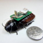
NCSU insectCyborg cockroaches may be the search-and-rescue teams of the future. The enhanced roaches can pinpoint the source of a noise using electric pulses delivered to their antennae, and then crawl towards it.

The insects are the work of Alper Bozkurt and his team at North Carolina State University in Raleigh. They have built two types of audio-sensing “backpacks” that can be strapped on to Madagascar hissing cockroaches.

One has a single high-resolution microphone that can identify sound sources fairly accurately. The other has a three-microphone array that gets a precise fix on the source using the amplitude information from each microphone.

Using a computer to integrate the data from a network of 10 to 15 insects, the cockroaches are then guided towards the sound source via automated electric pulses to their antennae. The nerve stimulation causes the insects to turn left or right, essentially by simulating contact with obstacles in front of them. Bozkurt presented the work at a conference in Spain last week. Watch a video of them crawling here.

Hacking cockroaches like this is nothing new. Bozkurt and his group have been working with them for the past five years, and last year a Kickstarter project made “RoboRoaches” commercially available for the very first time. But Bozkurt’s newest project moves the field into more practical applications. His team hopes the cyborg cockroaches may be used to find disaster victims, for example people buried under rubble in the aftermath of an earthquake.

“Cockroaches as a platform are certainly better in terms of performance than anything we are currently able to build, and that will remain true for many years,” says Shai Revzen at the University of Michigan in Ann Arbor. “But one of the problems with these approaches is that they work well in the lab, where there are no distractions, but are much more tricky to apply reliably in real-world environments.”

That’s why the next stage of Bozkurt’s research is to take the insects out of the lab – though not to a terrain as complex as a dense pile of rubble, as yet. Once the lab phase is complete, his team plans to use cyborg roaches equipped with geiger counters to search for leaks in nuclear power plants.

“There are a number of applications where we can get insect-bot sensors out into the field to collect useful information,” says Bozkurt. “But in the next five or six years, we think this project will be ready to be fully deployed under the rubble.”

Azeen Ghorayshi, New Scientist

Image: Eric Whitmire/NCSU

Alun Williams

Very few places left for Elektra Awards 2014

Elektra Awards table picThe Elektra Awards 2014 are just a few weeks away, and there are only a few places left. The event takes place on the 26th November at the Lancaster London hotel, W2 2TY, to discover who the 2014 Elektra winners will be.

You can either book online or contact John Richards on 020 8253 8678 or email john.richards@metropolis.co.uk.

The shortlists have been drawn up, online voting for the Product Innovation and Technology Blog awards have closed, and winners have now been selected. All that is left is to ensure your seat at the industry’s biggest night out of the year!

To help get you in the mood for the evening take a look at some pictures from the 2013 Elektra Awards.

Elektra Awards 1

Alun Williams

Power Integrations launches InnoSwitch

PI InnoSwitch

PI InnoSwitch

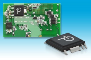
Today, Power Integrations announces  its InnoSwitch family of switcher ICs combines primary, secondary and feedback circuits into a single, worldwide safety-rated, surface-mount package.

“InnoSwitch ICs are the first switchers to combine the simplicity and low component count of primary-side regulation with the high performance of secondary-side control,” says Power Integrations vice-president Mike Matthews. “The InnoSwitch family’s high level of integration reduces power supply component count and its secondary-side regulated topology allows the use of simpler, lower cost, auto-wound transformers, yet improves production yield, resulting in significantly lower manufacturing cost. Two of the world’s leading mobile device makers are in production with chargers using InnoSwitch family ICs which incorporate FluxLink technology.”

InnoSwitch ICs will enable designers to exceed all global regulatory standards for efficiency and no-load consumption, claims the company, while minimising component count and providing accurate constant voltage and constant current up to 25W.

The InnoSwitch family is intended for use in smart mobile device chargers and adapters for a range of applications such as set-top boxes, networking equipment and computer peripherals.

Inside the device, secondary-side direct voltage and current measurements are communicated across the safety isolation barrier using high-speed digital FluxLink technology.

This proprietary feedback technique permits precise control without the need for a bulky optocoupler, Power Integrations says, without the performance compromises inherent in primary-side regulation (PSR), such as limited accuracy and efficiency and poor transient response versus no-load consumption.

InnoSwitch-based secondary-side regulated (SSR) designs are inherently less sensitive to the tolerance of external components such as transformers, diodes, resistors and capacitor,s the company says, which increases manufacturing yield and reduces total power supply cost.

Mobile device chargers up to  A can have a total component count as low as PSR designs, with accurate CV and CC control (±3% and ±5% respectively) and low voltage ripple.

InnoSwitch power-supply ICs include a high-voltage power mosfet, primary-side controller, FluxLink feedback technology and a secondary-side controller with synchronous rectification (SR). By combining the SR function with the secondary-side master controller and by leveraging the speed of the FluxLink communication channel, the SR switch timing is optimised for maximum efficiency.

The fast communication link also ensures reliable SR operation, eliminating shoot-through in either discontinuous conduction mode (DCM) or continuous conduction mode (CCM), even during transient loads and fault conditions. Effective SR operation in both DCM and CCM modes is especially beneficial in adaptive-voltage charger applications.

InnoSwitch ICs start up using bias current drawn from a high-voltage current source connected to the DRAIN pin, eliminating the need for external start-up components. An external bias winding reduces no-load and increases system efficiency during normal operation. The ICs also include comprehensive system-level features such as output over-voltage protection, overload power limiting, hysteretic thermal protection and frequency jitter to reduce EMI.

Samples are available now, priced at $0.59 to $0.78 in 10,000-piece quantities.

Reference design RDR-420 describes a 5V, 2A USB charger design and is available for download on the Power Integrations website.

david manners

IBM Unloads Chip Manufacturing Division

ARMONK, NY—IBM has dealt its chip manufacturing division to Globalfoundaries Inc. In an unusual move, IBM will pay Globalfoundaries $1.5 billion over the next three years to take over the division. As part of the deal, Globalfoundaries will also own and operate IBM's manufacturing facilities in East Fishkill, NY, and Burlington, VT.

Rohm voltage switcher for 42V

rohmRohm Semiconductor has introduced high voltage switching regulators with an extended operating temperature range of -40 to 105 deg C.

The BD9G101G DC/DC converter has an input voltage range of 6-42V. The internal high-side 42V power mosfet provides 0.5A of DC output.

The BD9G101G has a fixed 1.5MHz operating frequency allows the use of small inductors and ceramic capacitors. With a 45V/800mΩ internal power MOSFET that delivers greater efficiency, the BD9G101G delivers 0.75V±1.5% feedback pin voltage and integrates overcurrent protection, under voltage lock out and thermal shutdown functions.

A 6MHz synchronous step-down switching regulator, the BU9000xGWZ, has a low current pulse-frequency modulation (PFM) mode which provides up to 1.0A of load current with an input voltage range from 4.0V to 5.5V.


richard wilson