Sebastian Conran 3D printer built from weekly magazine

Sebastian Conran

Sebastian Conran

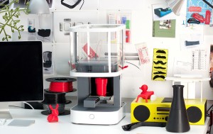
It is now possible to build your own 3D printer to make jewellery and smartphone cases in weekly installments.

It is the novel idea of Eaglemoss Collections which has teamed up with designer Sebastian Conran to create a 3D printer which can be built in weekly installments.

The publisher claims it will be possible to use the printer to make jewellery, games, figurines and mobile phone cases.

Weekly issues will be published to build the Eaglemoss’ Vector 3 printer, with software and a website which can be used to download designs featured in the magazines, along with specially customised software to run the printer.

Sebastian Conran, founding director of Sebastian Conran Associates said: “As 3D printing technology and applications become more mainstream, 3D printers are moving from the hi-tech workshop into the home, office and shed. Recognising this trend and opportunity, we worked with Eaglemoss to develop a 3D printer that was more suitable for home use.”

The website will also include a3D Create & Print Shop where userscan purchase a variety of different coloured plastics for their printer as well as a hostof additional printer tools.

Maggie Calmels from Eaglemoss said: “This collection also allows us to utilise our unique ‘partwork’ retail model; offering people the opportunity to purchase and build their own printer at small weekly costs, while the accompanying magazine is aimed at engaging readers and giving them the chance to learn more about the science behind the product.”

672f8c0ce947efa3e69f5c9341869314

richard wilson

Pop-up silicon 3D structures mimic biological structures

3D microstructures of device-grade siliconA way to make pop-up silicon structures which can mimic the shape of biological structures like the veins and brain cells has been found by researchers at Northwestern University, Illinois and the University of Illinois at Urbana-Champaign.

Complex three-dimensional (3D) structures in biology (e.g., cytoskeletal webs, neural circuits, and vasculature networks) form naturally to provide essential functions in even the most basic forms of life.

Compelling opportunities exist for analogous 3D architectures in human-made devices, but design options are constrained by existing capabilities in materials growth and assembly.

“We report routes to previously inaccessible classes of 3D constructs in advanced materials, including device-grade silicon,” say the researchers, “the schemes involve geometric transformation of 2D micro/nanostructures into extended 3D layouts by compressive buckling,” say the researchers.

Demonstrations include experimental and theoretical studies of more than 40 representative geometries, from single and multiple helices, toroids, and conical spirals to structures that resemble spherical baskets, cuboid cages, starbursts, flowers, scaffolds, fences, and frameworks, each with single- and/or multiple-level configurations.

Image: 3D microstructures of device-grade silicon - University of Illinois

david manners

Cambridge manufacturer makes LEDs shine bright

imagesCambridge Nanotherm is expecting to make a strong start to 2015 with growing sales of its nanoceramic thermal management products, particularly in the LED lighting market.

Cambridge Nanotherm installed its first production line last March.

“Upgrading our systems was necessary to cope with the demand,” commented Ralph Weir, CEO of Cambridge Nanotherm. “Many electronic and LED manufacturers are starting to realise the thermal benefits of working with nanoceramics, which are simultaneously cheaper than high-end “metal PCB” materials and higher performance.”

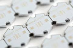
Cambridge Nanotherm’s patented process builds a nanoceramic layer on sheets of aluminium. The material is completed by a layer of copper, and can be converted into a PCB by established manufacturers.

“The nanoceramic layer acts as a dielectric with exceptional thermal properties, removing heat up to 20% more efficiently than the competition whilst also offering significant cost savings. The upshot is an affordable thermal management substrate / PCB material that outperforms everything else in its class,” said Weir.

Thermal management is used in high brightness LEDs remove heat from the assembly, which extends lifetimes of LEDs.


richard wilson

WaveJet Touch oscilloscope available from Amplicon

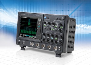
Teledyne-LeCroy-WaveJet-Touch-oscilloscopeThe Teledyne LeCroy WaveJet Touch oscilloscope is available from Amplicon.

The oscilloscopes come in either 350MHz or 500MHz bandwidth, 2GS/s sample rate and 5Mpts long memory.

The WaveJet Touch 350MHz model is priced from £3,625.

All channels on the oscilloscope can have active digital filtering, performing low-pass, high-pass and moving average filter operations, so unwanted frequencies are removed leaving only the desired ones. While the digital filters are active math trace functions can still be used for a more thorough analysis.

The options for signal acquisition include peak detect, where the maximum and minimum sample points are saved during two waveform intervals, as well as its corresponding waveform points. This is useful for viewing narrow pulses spaced far apart.

Each of these modes have an equivalent time sampling rate of 100GSa/s; automatic measurements can be made with 26 different parameters and min/max statistics, with up to four measurements being displayed simultaneously. The oscilloscope is also able to measure all occurrences of a parameter in a single acquisition.


richard wilson