STANFORD, CA—Researchers at Stanford University have increased the efficiency of a low-grade silicon solar cell by applying relatively cheap crystalline material, perovskite, on top of it.
New Material Boosts Efficiency of Solar Cells
STANFORD, CA—Researchers at Stanford University have increased the efficiency of a low-grade silicon solar cell by applying relatively cheap crystalline material, perovskite, on top of it.
New Material Boosts Efficiency of Solar Cells
STANFORD, CA—Researchers at Stanford University have increased the efficiency of a low-grade silicon solar cell by applying relatively cheap crystalline material, perovskite, on top of it.
New Material Boosts Efficiency of Solar Cells
STANFORD, CA—Researchers at Stanford University have increased the efficiency of a low-grade silicon solar cell by applying relatively cheap crystalline material, perovskite, on top of it.
New Material Boosts Efficiency of Solar Cells
STANFORD, CA—Researchers at Stanford University have increased the efficiency of a low-grade silicon solar cell by applying relatively cheap crystalline material, perovskite, on top of it.
AVX high CV wet tantalum capacitors match aqueous supercapacitors
AVX has introduced a series of high CV wet tantalum capacitors that the company says approach the ultra high volumetric capacitance densities of aqueous supercapacitors, as well as surmount their temperature and soldering limitations.
They are available on a 10- to 14-week lead-time.
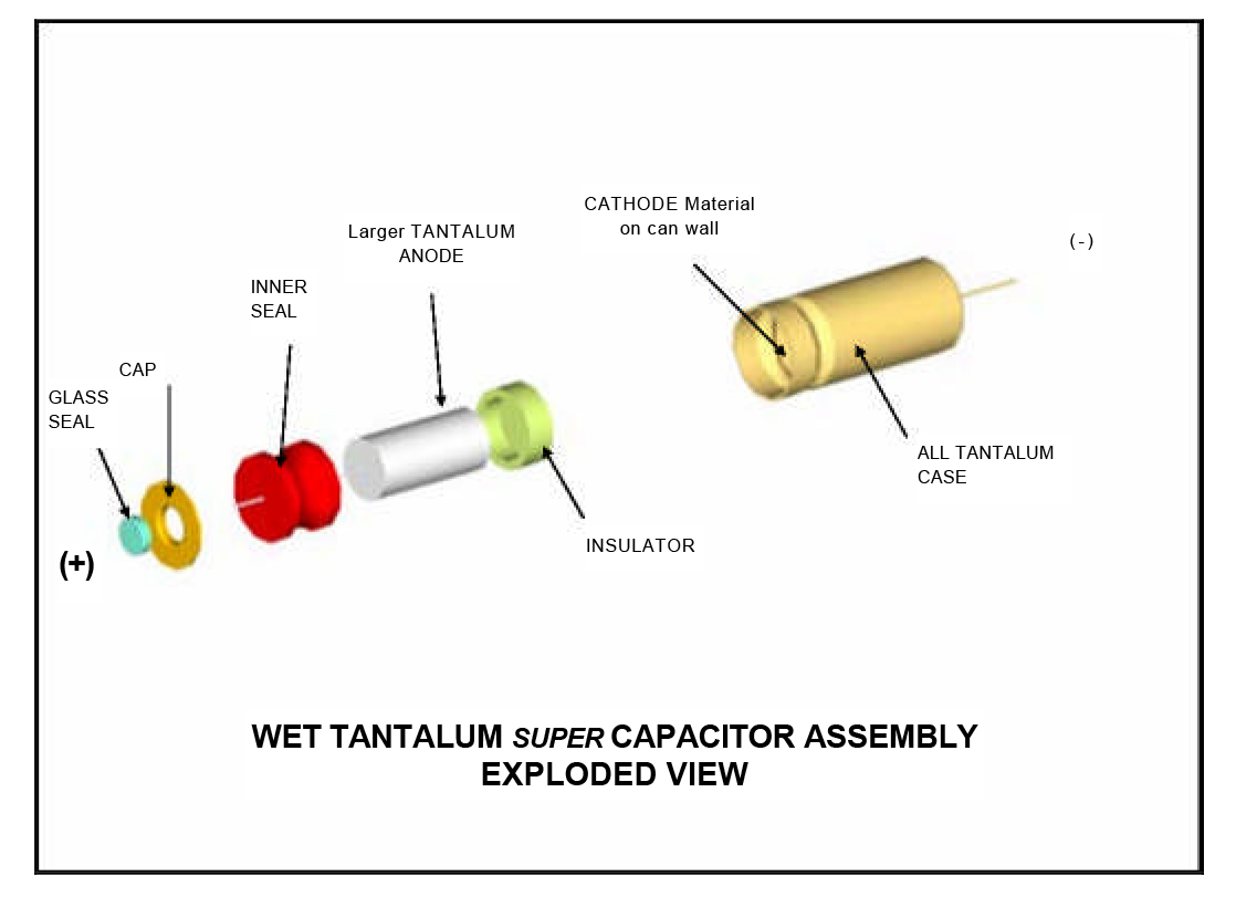 Developed using a design process based on high CV tantalum powders, the TWD DCUltraMax Series High CV Wet Tantalum Capacitors achieve high DC capacitance values and, unlike aqueous supercapacitors, are rated for continuous high temperature operation to at least 85°C and are compatible with both wave and reflow soldering to a PCB, according to AVX.
Currently available with a CV value of 50mF at 6.3V, TWD DCUltraMax Series capacitors are used in a variety of harsh environment applications, including: pulse applications, energy harvesting, energy storage, military electronics, and avionics.
Rated for use in temperatures spanning -55°C to 85°C, capacitance and voltage values for the new TWD DCUltraMax Series span 50mF to 150mF and 6.3V to 2.5V, respectively. However, series extensions exhibiting CV values of 150mF at 2.5V and rated for maximum operating temperatures as high as 105°C are currently in development.
In addition to high CV, TWD DCUltraMax Series capacitors also exhibit a low DCL of 0.0001CV, do not require derating, and are available with lead-free or SnPb terminations. Packaged in a DSCC T4 case (AVX’s E case), the series measures 26.97mm in length and 9.52mm in diameter without an insulating sleeve or 10.31mm in diameter with an insulating sleeve. The terminal welded to each case measures 57.15mm.
Comment: let’s move chip design a little to the left

Alex Duesener
Looking ahead to 2015 in the electronics industry, I see a shift left.
To explain, let me back up a bit. Whether it’s the automotive electronics segment, the internet of things (IoT), or mobile devices, the consumer now dictates design in a way he or she hasn’t historically.
Consumers of electronics technology now expect amazing new functionality each year, because we’ve delivered stunning electronics innovation for decades.
This has changed the nature of system design forever. The slow evolution away from partitioned design tasks and siloed teams has made the jump to hyper drive as design shifts left.
The Shift Left
What does this mean? Simply put, everything that was done “later” in the design flow must now start “earlier.” Software development needs to begin early enough to contemplate hardware changes (i.e., hardware optimization and hardware-dependent software optimization), while at the other end of the spectrum we see very early collaboration between foundries, electronic design automation (EDA) tool providers, and intellectual property (IP) suppliers to “co-optimize” the value proposition of each new process node.
This evolution’s essence is the examination of any and all dependencies in the product planning and development process to understand how they can be made to overlap in time.
Early software development helps enable software-driven verification methodologies. In turn, these methodologies are used to verify that the integration of sub-systems does not break the design, and that performance and energy can be optimized in the system context, with both hardware and software optimizations possible.
Numerous design processes are shifting left, but let’s take just one as an example: High-performance mixed-signal IP, such as DDR4 PHY in 16nm/14nm FinFET technologies, needs to be proven early in the process decision lifecycle. For this reason, foundries, EDA companies, and IP providers collaborate to make sure that critical IP blocks that will be needed by the first wave of process adopters are on early shuttle test chips.
Integration, Verification Evolution
The shift left also creates the need for faster subsystem integration and assembly along with retargeting of existing subsystems, the prototyping of new ones, along with performance, power, and area (PPA) analysis.
There are key changes in hardware verification too. The trend towards metrics-driven verification closure and unified verification methodology (UVM) continues proliferating at an accelerated pace. Verification IP (VIP) plays a critical role, in providing proxies for incomplete aspects of the system, as well as in proving adherence to interface standards.
While simulation remains the main workhorse for IP and subsystem verification, emulation has taken centre stage for system-on-chip (SoC) hardware verification, hardware/software integration, and operating system (OS) bring-up. Specialized hardware for emulation, acceleration, and prototyping is being applied by a much broader set of design teams to accelerate regressions and open the door to software-driven hardware verification methodologies.
In summary, the simultaneous and interrelated drives for faster time to market, product differentiation, and profit will all drive big changes in the way that electronics products will be designed in 2015 and beyond. Design teams shifting to the left will be the ones to reap big rewards and dominant shares in their markets as they do so.
Writer is Alex Duesener, corporate vice president for EMEA with Cadence.
Comment: Energy harvesting will be big in 2015

Dr. Wald Siskens, CEO of EnOcean
Energy is within reach everywhere, it just needs to be harvested: this is the principle of energy harvesting. Energy harvesting wireless solutions are already well established in the commercial building automation sector and for smart home systems. However, the technology is just getting started.
In 2015, new application fields for batteryless wireless communication will emerge to further enhance the world around us.
The “Forget Me Not” challenge at the end of 2014, a global design competition organised by the element14 community, gave us a taste of the technology’s possibilities. Engineers from around the world applied with their ideas for pioneering applications in the field of wireless monitoring and automation to perform tasks in our modern lives.
The projects included everything from a smart home security system to technology allowing users to take care of their pet remotely, to a system telling them if they’ve left laundry in the washing machine or to providing assistance systems for elderly people.
Most of these engineers were designing with energy harvesting wireless technology for the first time and this was no hurdle at all. On the contrary, the possibilities of sensors gaining their energy from the surrounding environment inspired many new ideas.
The flexibility of self-powering made the designers think about placing sensors in areas where data collecting devices that need maintenance or cables are not an option – a key parameter for the internet of things.
Powering sensors from the surrounding environment is not just a cool technology, it also ensures there is never any interruption in data collection needed to improve the interaction with our world.
Collecting and processing data opens up new possibilities for organising our daily lives independently from location and time. Thereby, data, collected once, can be reused for several applications. In a house, for example, the same system that saves energy based on the current room temperature, humidity, presence of persons and weather data also ensures a healthy comfort for the tenants or more security at home.
Batteryless sensors and switches are the assistants we need to collect and transmit the data. The tiny devices are indispensable for machine-to-machine communication, for efficient use of resources, for optimised sustainable agriculture or for demand-driven energy distribution.
Intelligent sensors, which monitor bridges, skyscrapers or dams, will lead to better sustainability of our constructions and save costs for future generations.
The intelligence to make use of the data can and will be implemented anywhere, but the systems that collect the initial information need to be reliable and perpetual so that we can “install and forget” this is where energy harvesting wireless sensors come in: the “things” in the IoT.
Writer is Dr. Wald Siskens, CEO of EnOcean
Top 10 technologies to transform the world

IoT (Photo: Intel)
Cloud computing/big data and 3D printing and (of course), the internet of things (IoT) are the three technologies most likely to transform the world during the next five years, according to technology market analyst IHS Technology.
These are the technologies which could change the world the Gutenberg printing press to the steam engine to the microchip.
So IHS Technology gathered its experts representing the technology supply chain from electronic components to finished products across applications markets ranging from consumer, media, and telecom; to industrial, medical, and power and them asked to nominate and vote for their top 10 most impactful technologies over the next five years.
The top three technologies were: 3D printing in third place, cloud computing/big data at No. 2, and little surprise that IoT comes out on top.
Total revenue for the 3D printing industry is forecast to grow by nearly 40% annually through 2020, when the aggregated market size is expected to exceed $35bn, up from $5.6bn in 2014.
IHS forecasts that global enterprise IT spending on cloud-based architectures will double to approximately $230bn in 2017, up from about $115bn in 2012.
The potential of IoT replies on predictions that more than 80 billion Internet-connected devices are projected to be in use in 2024, up from less than 20 billion in 2014.
The other key technologies identified by IHS Technology analysts were:
- Artificial intelligence
- Biometrics
- Flexible displays
- Sensors
- Advanced user interfaces
- Graphene
- Energy storage and advanced battery technologies
ARM challenges young engineers in California
![]() ARM has partnered with the Tech Museum of Innovation in San Jose, California to sponsor a video contest for the Tech Challenge 2015.
ARM has partnered with the Tech Museum of Innovation in San Jose, California to sponsor a video contest for the Tech Challenge 2015.
The contest is open to boys and girls in grades 4-12 to make a video of how they tack real-world problems using engineering-design thinking.
The annual two-day event tests skills such as creativity, problem-solving and design. It also helps participants to deal with risk-taking and teaches them how to learn from failure and perseverance.
This year’s challenge, which takes place on April 25 & 26, is to build an earthquake-safe structure.
Videos may record the design brainstorming process or simply chart the project as a whole. The films will be judged on creativity, visual and audio appeal and storytelling. The top three videos will receive an award and be played during the event.
Where: The Tech Museum, 201 South Market Street, San Jose, Calif., 95113
When: Contest final dates:
· Saturday April 25, 2015, Grades 4-6 and 9-12
· Sunday April 26, 2015, Grades 7-8.