Dyson is on fast electronics trajectory

 From being a small part of the traditional vacuum cleaner to defining the product itself with the latest robotic vacuum cleaner, Dyson is placing electronics at the heart of its product development plans.

As a result the consumer products company is dramatically expanding its electronics hardware and software development teams and it is building a new R&D centre in the UK to support the growing electronics design activity.

Dyson is a global brand which has reputation of innovating domestic vacuum cleaner design.

There was not much electronics in the original vacuum cleaners. As a result electronics design played a minor role in the development of the first Dyson products.

But all this has changed in 2015 with the launch of the Dyson 360 Eye robot vacuum cleaner. Electronics is not only part of the design; electronics defines the product.

Dyson is one of the companies planning to use artificial intelligence and robotics to bring a new level of intelligent computing to the home.

“We have the mechanical and software capabilities, but we still lack understanding – machines that see and think in the way that we do. Mastering this will make our lives easier and lead to previously unthinkable technologies,” says company founder, Sir James Dyson.

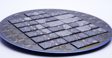
Electronics hardware and software design has become an important element in product development at Dyson.

So much so that the company is planning to create a new electronics development centre at its facility in Wiltshire, and the consumer company has a programme to expand its electronics hardware and software development teams significantly this year.

“If we look back at Dyson products over the last 20 years, there was not a lot of electronics in the early vacuum cleaners,” points out Claudio Zizzo global head of electronics at Dyson.

This changed with newer products such as the company’s cooling and heating fans.

“Electronic systems were incorporated for advanced motor control to optimise energy consumption and reduce motor acoustic noise,” explains Zizzo.

“Sir James Dyson was quick to recognise that electronics was no longer just an enabler within the product. With the 360 Eye robot, it is the product,” says Zizzo.
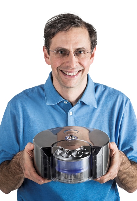
Claudio Zizzo

Claudio Zizzo

Zizzo, who has strong background in managing electronics design groups at Motorola and Rolls-Royce, was recruited by Dyson almost two years ago to build up the firm’s team of electronics hardware, system and software development engineers.

“The company recognised that electronics was becoming a core element of future product development plans,” says Zizzo.

Dyson is making a major investment to expand its electronics development capabilities.

“In the consumer world the pace of development is very aggressive. Dyson is developing electronics technology on a very fast trajectory and we see a big opportunity to innovate,” says Zizzo.

A new robotics laboratory, which the company is building at its Wiltshire headquarters will open in next two months. The company is in the middle of a recruitment programme which will add hardware, software and systems engineers to its development teams.

Dyson has recruited 60 electronics development engineers in the UK in the last 12 months and Zizzo says there are plans recruit another 70 engineers this year.

The company is looking for engineers with a range of skills and experience. “We are looking for graduate engineers, but also experienced engineers and team leaders,” says Zizzo.

Dyson has also collaborated with Imperial College in the creation of a robotics R&D laboratory at the London university.

With research at the Dyson Robotics Laboratory at Imperial College London, which represents a £5m collaboration between the College and the manufacturer, Dyson is looking to apply the operation of robots beyond controlled environments, such as assembly lines where they work within a strict set of parameters.

The idea is that robots could successfully navigate the real world by interacting safely with their surroundings. To do this it is necessary to develop robots that can process visual information in real-time.

The Dyson 360 Eye has a 360 degree camera and many tens of sensors which are used to model the robot’s environment in 3D. 
The goal is for robots not only to determine the layout of a room, but also distinguish between objects and determine their purpose.

Each house is different, points out Zizzo, so the robot must carry out probabilistic and heuristic analysis of the images and sensor data in real-time, which requires high performance digital signal processing and sophisticated software algorithms.

“A lot of learning takes place in the robot with the aim of getting maximum floor/area coverage with the minimum run time,” says Zizzo.

The electronics design activities within Dyson incorporate analogue and power circuit design as well as embedded processor systems design. There is advanced motor control for the four drive motors in each robot, for example as well as radio frequency circuit design for the Wi-Fi system.

Dyson is also developing its own software to control and operate the robot. The software development team numbers 55 people and is growing rapidly.

The software and connectivity team is also responsible for the development of the smartphone apps which are used to operate the robot.

The company which has expanded its horizons from vacuum cleaner design to robotics is not planning to stop looking for new areas in which it can innovate.

Last November, Dyson announced its plans for a £1.5bn investment for future technologies, including a £1bn for the research and development of new product technologies.

Zizzo believes electronics design will become a major element of future product development at the company.

“The products that come after this first robot will have even greater levels of electronics within them,” says Zizzo.
“There is an electronics revolution taking place at Dyson,” says Zizzo. “I believe that anyone joining the company now is joining Dyson at a very exciting point in time.”

Richard Wilson

An Intel PC in a stick

Hannspree Micro-PCClaimed to be the smallest PC ever, Hannspree has squeezed a real Intel+Microsoft PC into a stick – it includes a quad-core Atom and will run Windows 8.1.

Called Micro-PC, in needs to be plugged into an HDMI-compatible display (touch optional) and a wireless keyboard with tough pad.

“Set up office in any location and be up and running in less than 2 minutes,” claimed the firm.

It is not quite as tiny as a memory stick and, at 11cm long and 38g in weight, it might need a little support when inserted directly into horizontal HDMI ports.

Hannspree Micro-PC other sideIn the stick is a 1.83GHz quad-core Atom, 2Gbyte RAM, 32Gbyte eMMC flash, 802.11b/g/n Wi-Fi, Bluetooth 4.0, a Micro USB port, a USB2.0 port, and a Micro SD card reader.

The graphics engine is clocked at 311MHz, or 646MHz in burst frequency mode for gaming and multimedia.

“Just load it up with digital content and slip it in a pocket to take large presentation files, HD video and personal data anywhere,” said Hannspree. “The architecture has been adapted to make optimum use of the Windows 8.1 operating system.”

The Micro SD slot officially supports up to an additional 64Gbyte of storage “but has been successfully tested with up to 128Gbyte – around 80 movies”, said the firm.

It is also marketing the stick as an all-in-one PC bundle with a number of HannsG’s touch screen displays – see below.

Hannspree Micro-PC sideAt a glance

  •  Windows 8.1 pre-loaded (English, German, French, Spanish, Italian)
  • Quad core 1.83GHz Intel Atom Z3735F (2M cache)
  • 2Gbyte RAM
  • 32Gbyte internal flash card (24.8Gbyte free)
  • 802.11b/g/n Wi-Fi
  • Bluetooth 4.0
  • Micro USB
  • USB2.0
  • Micro SD card reader
  • 111x38x10mm
  • With: HDMI cable, charger
  • 38grams

Suggested all-in-one option

  • Paired with HannsG’s HT231HPB monitor
  • 23in screen – (TN, not IPS)
  • 10 point touch
  • 250cd/m2
  • 1000:1 contrast (enhanceable)
  • 1920×1080 (16:9)
  • 5ms typical response
  • 170°/160° H/V viewing
  • VGA, HDMI, DVI (HDCP) inputs
  • 575x408x44 (d)
  • Built-in speakers
  • 100x100mm VESA mount


steve bush

Software documents Linux activity live

undo3Linux programs to make a detailed recording of themselves as they run, claimed Undo Software of Cambridge as it announced a product called Live Recorder.

“Until now, in order to solve a problem reported on code running in production, developers have needed to gather information relating to the failure to write a test case and, or, reproduce the bug in-house,” said the firm. “Recording enables developers to debug an exact copy of the original program’s execution, allowing them to track down bugs without needing to reproduce them in-house, write test cases, or make visits to customer sites.”

The recorder creates an ‘Undo Recording’ of a failure which can be sent back to developers by the user.

Feeding this into the firm’s reversible Linux debugger (UndoDB, specially configured) allows it to reconstruct programme activity, said Undo, including every memory access and every instruction executed.

“Developers can rewind and replay their code to find bugs,” explained the firm.

The recorder comes in the form of a library that can be embedded within a programme. This library has a C API that allows recording to be started and stopped, and a recording to be saved to a file – either on demand or automatically on termination of a program – in case of a program crash, for example.

When recording is not enabled, the software is “completely dormant”, according to Undo.

Live Recorder is available now and supports compiled programs on 64-bit x86 Linux distributions. Licencing allows software vendors to re-distribute the library with their programme.

steve bush

Prolonged IC industry upswing ahead, says Future Horizons

Malcolm Penn - Future Horizons

Malcolm Penn – Future Horizons

It is time to prepare for one of the strongest and longest upswings in the semiconductor industry’s history, it was stated at the Future Horizons’ IFS 2015 forecast meeting in London this morning.

“Every single duck is lined up for the industry to go into a prolonged market upturn,” said Malcolm Penn, CEO of Future Horizons.

The industry grew at 9.9% last year and ASPs have been rising for seven consecutive quarters and there have been twelve successive quarters of unit demand growth, said Penn.

“People don’t believe it,” said Penn, “it doesn’t fit with what they want to believe.”

One problem is that “too many people are talking the industry down,” said Penn instancing the SIA forecasting 3.4% industry growth in 2015 and 3.1% in 2016, “hardly a vote of confidence from the industry’s advocate,” commented Penn.

Other factors mandating the upswing are currently high fab utilisation rates, low levels of capex and negligible inventory builds. The auguries all point one way but the industry idn’t acting on them.

The ‘I want one more quarter syndrome’ is deeply embedded in peoples’ psyche, said Penn.

The macro indicators are also above the long-term trend. This week’s IMF GDP forecast is for 3.5% growth this year and 3.7% growth next year which are both ahead of long-term world GDP growth of 3.4%. In 2011-4 GDP growth was an above average 3.5%.

So the Future Horizons forecast for this year is for healthy 8.5% growth which will deliver an industry with $1 billion sales per day – $364 billion for the whole of this year.

If the 2014 recovery trend holds steady, however, the growth could hit15%, said Penn.

david manners

Sub-threshold operation for lowest MCU power

Ambiq ApolloSub-threshold transistors have allowed a 32bit ARM Corex-M4F microcontroller to run at 35µA/MHz, and sleep at 100nA with the real-time clock (RTC) running.

Announced by University of Michigan spin-out Ambiq Micro, it uses technology invented at the University and developed through collaboration foundry giant TSMC.

Sub-threshold operation – where low supply and gate voltage means mosfets are either ‘off’ or partially ‘on’, but never fully on – is a known route to low power consumption, as power scales with V2, but is also a known route to chips that are hopelessly sensitive to process and temperature variation.

Ambiq has a contrary view: that sub-threshold can be made to work in mass production, and put money on it. In 2013 the firm released stand-alone sub-threshold RTC chips that consume only 55nA. “The RTC was a stepping-stone to prove it is real technology because people were in disbelief,” Ambiq v-p of marketing Mike Salas told Electronics Weekly.

Salas points out that Swiss watch companies were using sub-threshold chips years ago, but they only had 5-10 hand-crafted transistors. Ambiq’s mission, and that of the University before, has been to find a way to make reliable sub-threshold chips on a big scale using industry standard processed and cad tools.

According to Salas, one hurdle on the way to sub-threshold chips was that transistor models provided by foundries did not extend accurately into the sub-threshold region. To push the envelope to lower voltages “it took 5-6 years, a lot of information gathering, a lot of test chips, a partnership with TSMC, and a lot of modelling work”, he said.

From this came not only better models, but digital and analogue circuits specifically for sub-threshold transistors.

How these work remains secret. “The circuits are very dynamic, very adaptive, and compensate for bad effects,” is all Salas would say.

Research has shown sub-threshold operation is not suitable for all parts of a chip.

In the microcontroller, dubbed ‘Apollo’, “there is intelligent partitioning on where to provide sub-threshold and when not”, said Salas. “A couple of places have standard super-threshold transistors, there is a big chunk of near-threshold, and in other areas there is real sub-threshold, down to 0.5V.”

Now it is working, would the firm licence its technology?

“A lot of people have asked, and ‘no’ is the basic answer,” said Salas. “But we do want to licence it to ancillary chip makers – very selectively. For example, if radios out there are minimising our value in a solution.”

This broader approach to energy reduction could well be extended to software and compilers which, according to Salas, need to be designed for energy rather than code size or performance.

Ambiq Apollo performanceApollo is implemented on TSMC 90nm CMOS. This was chosen simply because it was the finest geometry available with embedded flash, said Salas, and was nothing to do with sub-threshold performance or leakage. “If you were implementing purely for sleep power, you would go for 180nm, at the expense of much higher active power,” he said, adding that Apollo doesn’t have a leakage problem, borne out by the 100nA in sleep+RTC figure.

Ambiq has also said, without further explanation, that leakage current of ‘off’ transistors is used to compute in both digital and analogue domains.

Why chose to implement an ARM Cortex-M4F rather than the smaller but less potent M0.

“The power delta between M0 and M4 is so small, and the M4 will execute faster and so shut off more quickly,” said Salas.

The Cortex-M4 is an M3 plus DSP extensions.

Energy Micro, the previous record holder for energy efficient MCUs (and now part of Silicon Labs), had similar arguments for adopting Cortex-M3 rather than M0 for its first product, although eventually added a parallel M0 family.

The F in M4F indicates the CPU has floating point extensions. “This is tremendously valuable for the IoT where sensors are on all the time. Floating point helps with the analytics algorithms,” said Salas. “The other bonus is that customers who use Matlab generally have to take the code and convert to fixed-point for smaller code and lower energy. We save customers the float-to-fixed conversion.”

As well as the core, sub-threshold techniques have been applied to both analogue and digital peripheral domains in Apollo. “Our power floor is just so much lower than competitors,” claimed Salas. And like those competitors, Ambiq has optimised its peripheral architecture for power saving. “We all play the same architectural games, like deep FIFOs to avoid turning on the core,” he said.

Including two on-chip dc-dc buck converters, Ambiq is claiming 840µA at 24MHz (top speed, 35µA/MHz) running a CoreMark from flash at 3.3V. “We didn’t cheat on the headline number. It is a real CoreMark running out of flash. I could quote a much lower figure running out of RAM,” Salas added.

At 3.8V, this improves to 32µA/MHz. Sleep with RAM retained is 130nA at 3.3 or 3.8V, or 100nA at both voltages with no RAM retention.

Although core voltage is low, external pins work like any other MCU. Said Salas: “It looks and feels like any other microcontroller – the magic is inside the chip, all power and voltage converted.”

Wake from sleep is 10us with the RC oscillator clock.

Silicon samples are with Ambiq and “power numbers look great,” said Salas.

There are to be four Apollo MCUs, all with the same peripherals, differing only in memory: 64-512kbyte flash and 16-64kbyte RAM.

Peripherals include: 10bit 13channel 1Msample/s ADC, ±2ºC temperature sensor, voltage comparator, x8 SPI master, x2 I2C master, SPI/I2C slave, UART, RTC, clock oscillators (LF RC, HF RC, XTAL) and x8 timers.

Operation is over 1.8 to 3.8V and -40 to 85ºC.

Package options will be 4.5×4.5mm 64pin BGA with 50 GPIO pins, or 2.4×2.77mm 42pin chip-scale with 27 GPIO.

Volume production is scheduled to commence in the spring.


steve bush

Linear Tech CEO: industrial market growth “relentless”

Lothar Maier

Lothar Maier

Over the past year, we continued our focus on the automotive, industrial and communications markets. We addressed each with analogue and power solutions to help our customers get to market faster and more reliably.

In the automotive market, fuel efficiency, comfort, navigation/entertainment, and safety drive the need for new analogue solutions.

Many of the mechanical functions in an automobile are being converted to electronic to reduce weight, improve fuel economy and increase reliability. The recent introductions by nearly every automobile manufacturer of hybrid and electric vehicles highlight this trend, and show how electronics are reshaping the automotive market.

The transportation market is our second largest end market, as well as the company’s fastest growing market.

Our largest market is industrial and its growth is relentlessly driven by the need for ongoing innovation.

Our industrial efforts span factory automation and process control, scientific instrumentation, medical and security, among others.

This market demands better efficiency, more automation, greater precision and higher integration, a cycle that started 10 years ago and today shows no signs of slowing.

Looking to the year ahead, I am encouraged that our customers in UK, Europe and other parts of the world continue to seek new design solutions.

I continue to be optimistic about the opportunities in the year ahead.

Lothar Maier, CEO, Linear Technology  

Richard Wilson

Consolidation on the cards for UK mobile operators

Apple iPhone 5S

Following the purchase of EE by BT, the UK mobile market may see a consolidation of carriers with 3 taking over O2.

O2 is owned by Spanish network operator which is struggling with heavy debts. Telefonica was in negotiations with BT about possible sale but any deal fell through when BT chose EE.

3 is owned by Hutchison of Hong Kong which is owned by Li Ka-shing.

3 is expected to have to pay $13.6 billion to buy O2.

A combined 3 and O2 would be the UK’s biggest mobile operator with 31 million subscribers.

An alternative option for Telefonica is to IPO O2.

david manners

Sebastian Conran takes 3D printing into schools

Sebastian Conran

Sebastian Conran

Sebastian Conran has teamed up with publisher, Eaglemoss to bring 3D printing and design into the school classroom.

The Vector 3 printer comes with a step-by-step 3D design tutorial course for school learning.

Sebastian Conran, founding director of Sebastian Conran Associates, said: “As 3D printing technology and applications become more mainstream, 3D printers are moving from the hi-tech workshop into schools, the home and the office.”

Using the Vector 3 in conjunction with the software course will allow students to create a range of objects, including models for science subjects such as cells and molecules.

Maggie Calmels, senior v-p at Eaglemoss, believes that 3D printing allows for a new and “creative approach to teach STEM and design subjects and it is great to be amongst those that are paving the way in making 3D printing available to a wider audience.”

To assist schools with purchasing the product, Eaglemoss has developed a multi printer pack of up to six printers specifically for schools’ supply, plus a schools retail pack of one printer which comes with associated design projects and easy to follow 3D design course for in classroom teaching.

A dedicated website area has also been set up for schools.*

Eaglemoss has also launched the 3D printer as a partwork collection which can be built in weekly installments.

The company is also setting up a 3D design competition for students which will be judged at the Design Museum in June 2015. Prizes include a Vector 3 printer as well as a donation to the winning school’s technology budget.

Richard Wilson

Comment: Product-centric design is the right approach

Bob Potock

Bob Potock

For as long as many of us can remember, the PCB has been at the centre of the product design process.

This PCB-centric design approach is characterised by PCB, mechanical and supply chain teams working in silos until the all the pieces come together at the prototype stage. If something doesn’t fit or a cost target is missed, recovery is expensive.

It’s an approach that has worked reasonably well over the years; but product composition is changing and 2014 saw a marked shift to a product-centric design approach that I expect to see a lot more of in 2015.

Let’s consider system-on-chip (SoC) ecosystems and product packaging. The SoC has had a profound impact on the hardware design process.

With so many functions being consolidated on a single chip and application specific flavours of the SoC, engineers can make use of reference designs. Many products use SoC reference designs with an added special sauce for differentiation.

Product packaging or form factor, on the other hand, has become an important competitive factor and we’re seeing ever more complex shapes and angles.

Consumers are looking for smaller and cooler looking products. This translates into smaller PCBs fitting into smaller enclosures with less room for error.

On one hand, SoC-based reference designs make the hardware design process easier, but those designs still need to fit within a very creative enclosure demanding much closer collaboration between design disciplines.

For example, the enclosure may dictate a two-PCB implementation versus a single board design. Such PCB planning is intrinsic to product-centric design.

This is a big task for current-generation, single PCB 2D design tools. Their limitations include the lack of product-level design visualisation; lack of multi-board support; and limited or no MCAD co-design capabilities, concurrent design support, or cost and weight target analysis.

A multi-disciplinary and collaborative product-centric design process is a profoundly different approach. This is being driven by changing competitive factors and a PCB-centric methodology simply can’t keep up. This changing environment requires a more collaborative and responsive design process.

One key product-centric design feature that allows companies to quickly respond to new and complex product requirements is architectural validation. This is the bridge between the product requirements and detailed design – and it’s an area where companies can achieve a competitive edge for their products if they get it right.

Before detailed design, a multi-discipline analysis of the requirements versus the proposed product architecture is done.

Factors are reviewed such as: size, weight, cost, shape and functionality of the new product; how many PCBs are needed and whether they’ll fit in the enclosure.

Other reasons manufacturers are achieving cost and time savings with product-centric design include:

  • Concurrent 2D/3D multi-board design planning and implementation
  • Import/export of STEP models with clearance and collision checking
  • The use of modular design (design reuse)
  • Improved communication with the supply chain

These capabilities support product-level considerations and enable companies to maximise their competitive edge.

Writer is Bob Potock, vice president of marketing, Zuken.


Richard Wilson

Will 2015 be the key year for graphene?

imec wafer scalingGraphene has yet to move out of the research lab, but 2015 could be the year we see the first devices using the “new” semiconductor material.

Imec has developed the industry’s first integrated graphene optical electro-absorption modulator (EAM) capable of 10Gbit/s modulation speed with a very low insertion loss and drive voltage.

For chip-level optical interconnects, graphene will be used for its fast tunable absorption over a wide spectral range.

Imec is also developing a scalable, manufacturable silicon-based optical interconnect technology for telecoms applications.
Researchers at IBM have used graphene in a re-usable substrate for making blue LEDs.

“In principle, graphene has been demonstrated as an infinitive source for growing these [GaN] semiconductor materials, making the work an enormously cost-effective and reliable production method for single-crystalline films,” said IBM scientist Dr Jeehwan Kim.

“Growth of a 4 inch, wafer-scale GaN film would require a 4-inch SiC wafer at the cost of some $3,000. Now, graphene can be produced in a lab to replace the expensive SiC wafer,” said Kim.

Graphene NanoChem, the Malaysia-based graphene company, has announced a product development agreement with Sync R&D for graphene-enhanced lithium-ion batteries for use in electric buses

The Li-ion battery is anticipated to be a critical component for electric vehicles as a fully charged battery will enable the bus to travel between 180 and 200km before requiring to be recharged.

A graphene-enhanced anode in the Li-ion battery is claimed to provide 10 times more power storage and significantly reduces the time required to recharge the battery.

Richard Wilson