Design kit for STM32F7 MCU has Arduino extension

Design kit for STM32F7 MCU

Design kit for STM32F7 MCU

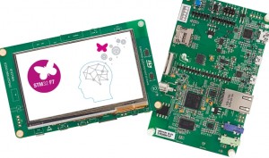
STMicroelectronics’ STM32F7 series ARM Cortex-M7 core microcontroller just got easier to design in with a starter kit that has a Arduino Uno connector for coupling into the open source design environment.

Dubbed the Discovery kit, it comes with a 4.3-inch WQVGA colour LCD with touchscreen.

There is a 128Mbit Quad-SPI flash memory interface, 128Mbit SDRAM and interfaces for a micro SD card socket, Ethernet and USB OTG HS connector.

There are audio inputs and outputs, a camera connector and MEMS microphones.

The kit is available from distributor Rutronik which is also selling two versions of the STM32F7 MCU evaluation board. The STM32746G-EVAL2 and the STM32756G-EVAL2 with hardware cryptography acceleration.

The evaluation boards have a 5.7-inch touchscreen, 32Mbyte SRDRAM, the camera module and the RTC with backup battery.

The STM32F7 MCU with on-chip accelerator achieves 1082 CoreMark at 216MHz.

A version of the MCU, STM32F756, incorporates a crypto/hash processor providing hardware acceleration for AES-128, -192 and -256 encryption with support for GCM and CCM, Triple DES, and hash (MD5, SHA-1 and SHA-2) functions.

The series can be ordered at distributor Rutronik in seven different packages with 100 to 216 pins and as small as 4.5 x 5.5mm in WLCSP.


Richard Wilson

Concept Engineering upgrades netlist debugger for complex SoCs

Concept Engineering SpiceVision

Concept Engineering SpiceVision

German chip debugging tool firm Concept Engineering has released its latest generation tools.

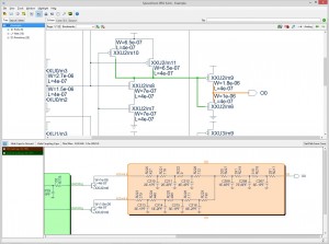
StarVision PRO, RTLvision PRO, GateVision PRO, and SpiceVision PRO are scriptable debugging and visualisation tools.

As well as a debug tool for  analogue, digital and mixed-signal designs, StarVision PRO provides customisable design rule checks and automated netlist pruning.

There is an RTL debugger, RTLvision PRO, and GateVision PRO can be used for netlist debugging of more complex SoC netlists.

For SPICE simulation, the SpiceVision PRO can be used to view and debug transistor-level and post-layout netlists.

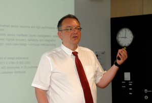
“With version 6, we continue to improve our specialized product family with individual tools for specific circuit debugging problems,” said Pascal Bolzhauser, product manager for Concept Engineering′s Vision product line.

Other features include:

  • StarVision PRO now also allows netlist pruning for the most common post-layout formats, DSPF and SPEF.
  • Improvements in the database API and GUI API allow even more sophisticated code to be developed and executed by the tool.
  • Enhanced batch processing capabilities allow more efficient processing of user-defined analysis and debugging tasks.
  • Unified File Open Dialog to load complex mixed-language SoC designs and libraries.

Version 6.0 products are available now to download from the company′s website. There are no additional fees for existing customers with valid licenses.

Richard Wilson

Golf loss is solar farm gain in Japan

Impression of Kyocera Kanoya Osaki Solar Hills Old golf course land in Japan is to become a solar farm, according to Kyocera, which is working with partners on the conversions.

The most recently announced is a 23MW power plant on an abandoned golf course in Kyoto Prefecture, which will generate an estimated 26GWh/year.

“Over-development of golf properties during the real-estate boom of the 1990’s and 2000’s has led to hundreds of idle courses today that are now under analysis for repurposing or redevelopment,” said Kyocera.

Earlier this year, the firm revealed a partnership to construct and operate a 92MW solar farm on a site stretching across Kanoya City and Osaki Town in Kagoshima Prefecture – selected for golf course construction more than 30 years ago, but abandoned. 340,740 Kyocera solar modules will cover 2,000,000m2 and generate around 99GWh/year.

Kyocera 23MW solar farm site“In the United States, several cities in states such as Florida, Utah, Kansas and Minnesota are having public discussion and considering proposals on how best to re-purpose closed golf courses,” said Kyocera.

Above: What the 92MW Kanoya Osaki Solar Hills Solar Power Plant might look like.
Right: Abandoned golf course to become a 23MW solar farm.

steve bush

NXP sells CMOS sensor business to ams

Thomas Riener - AMS - Executive Vice President General Manager Full Service Foundry - Executive Vice President Marketing Communications

Thomas Riener, ams,executive vice president

NXP has sold its CMOS sensor business to Austrian mixed-signal chip firm ams.

NXP is currently in the middle of a merger with US chip firm Freescale Semiconductor.

Earlier this summer NXP also agreed to sell its RF power business to Chinese private equity firm Jianguang Asset Management  for $1.8bn.

The sale of the RF power business, which supplies RF power amplifiers to the mobile phone basestation market, seems to have been a element in the proposed merger of NXP with Freescale Semiconductor.

Proceeds from the sale of the RF Power business will be used to partly fund the acquisition of Freescale.

Now the sensor business, which includes humidity, pressure and temperature sensors, is to be sold to ams for an undisclosed amount.

According to Thomas Riener, executive vice president, marketing and strategy at ams:

“The acquisition of NXP’s CMOS sensor business expands our existing environmental sensor technologies and is a synergistic addition to our chemical sensor capabilities and smart lighting solutions. This portfolio makes ams the one-stop shop for environmental sensors.”

Ams is already has its sensors designed into smart phones and it is looking to expand this to wearables, smart buildings and medical markets.

It is looking to develop integrated sensor devices combing a processor, wired and wireless interfaces and power management.

“Environmental sensors can replicate and enhance human responses by monitoring and measuring smell, pressure and temperature. By capturing this information electronically, data-driven decisions can be made automatically and efficiently,” said Riener.

The new additions to the environmental sensor product portfolio are available for customer sampling now. Temperature and relative humidity sensor solutions will be in mass production early in 2016.

Richard Wilson

Maxim quad deserializer for ADAS

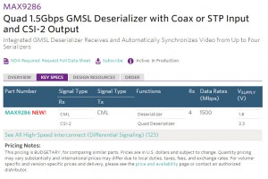
maxim-9286The MAX9286 quad deserializer from Maxim enables the design of surround-view systems for ADAS.

One MAX9286 gigabit multimedia serial link (GMSL) deserializer receives and automatically synchronizes video from up to four cameras.

Surround view systems are a key component in today’s emerging ADAS market. The MAX9286 automotive deserializer accepts and synchronizes video streams from four cameras via a shielded twisted-pair (STP) or coaxial cable by up to 15 meters.

The MAX9286 outputs the data via a four-lane, industry-standard CSI-2 interface to a video processor.

It reduces board space and component count by replacing four discrete deserializers and an FPGA.

Inaddition, the deserializer eliminates additional software required for camera synchronization.

The MAX9286 is suitable for machine vision and 3D-camera systems.

Features

  • For Multicamera Stream Applications
    • Works with Low-Cost 50Ω Coax Cable and FAKRA Connectors or 100Ω STP
    • Data from Image Sensors Are Synchronized to the Same Pixel
    • Automatic Internal/External Generation of Camera Sync
    • Equalization Allows 15m Length Cable Operation at Full Speed
  • Multiple Input/Output Features for System Flexibility
    • 1 to 4 Lane CSI-2 Output with 80Mbps to 1200Mbps Per Lane
    • Swappable/Selectable Serial Input/Output with Swappable Polarity
    • 9.6kbps to 1Mbps Control Channel in UART, Mixed UART/I²C, or I²C Mode with Clock Stretch Capability
  • Peripheral Features for System Power-Up and Verification
    • Built-In PRBS Tester for BER Testing of the Serial Link
    • Programmable Choice of Nine Default Device Addresses
    • Two Dedicated GPIO Ports
    • High-Immunity Mode for Maximum Control-Channel Noise Rejection
  • Meets Rigorous Automotive and Industrial Requirements
    • -40°C to +105°C Operating Temperature
    • ±8kV Contact, ±20kV Air ISO 10605 and ±8kV Contact, ±12kV IEC 61000-4-2 ESD Protection

david manners

Interview: Making the BBC Micro:bit Bluetooth Smart

Martin Woolley, Bluetooth SIG Technical Program Manager

Martin Woolley, Bluetooth SIG Technical Program Manager

Bluetooth Smart is a key element of the Micro:bit, the BBC’s much heralded educational computing device aimed at Year 7 children in the UK. Electronics Weekly talks to Martin Woolley, Bluetooth SIG Technical Program Manager, who led the work around Bluetooth, including creating a specific Micro:bit Bluetooth Profile…

Q: You must be pleased with the launch of the BBC Micro:bit and its embracing of Bluetooth Smart?

A: Absolutely. One million UK school kids will be receiving a BBC Micro:bit and for many of them this will give them their first taste of coding and of Bluetooth Smart too. We’re really excited about this!

Q: Being an educational initiative, everyone must wish it well and hope it makes an impact on the UK?

A: I should think so, yes. The word “strategic” gets bandied around a lot these days but the whole SIG believes this is one occasion where it’s right and proper to use it. We really think that this is an initiative that has strategic significance for the UK and it will hopefully help plug our apparent skills gap and pave the way for a new generation to embrace and drive forwards the Internet of Things.

I trace my career back to the day my form teacher brought a Commodore Pet microcomputer into school one day and right there and then a geek was born! I’m certain in the future we’ll hear young, British technology leaders saying that they first got interested in technology when they were given a BBC Micro:bit at school.

Micro:bit Collaboration

Q: To what extent was the Bluetooth SIG involved in the design?

A: We designed a Bluetooth Smart profile specifically for the BBC Micro:bit so it can be used “out of the box” right away. It’s an important part of the overall blend of technologies that make up the Micro:bit since it’s the part that enables the Micro:bit to communicate and connect to other Micro:bits, devices, phones, tablets, cameras and everyday objects all around.

Q: Was it just you, or a team?

A: It was a team covering various aspects of the project. I designed the profile in consultation with other Micro:bit partners, through a series of face to face workshops which the BBC ran. Others from the Bluetooth SIG took care of things like contracts, Bluetooth SIG membership and the process of getting the Micro:bit through the qualification and listing process.
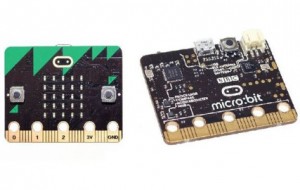
The BBC Micro:bit, front and back

The BBC Micro:bit, front and back

Q: Who exactly did you work with? Samsung? Lancaster University?

A: Samsung, ARM and Lancaster University. And the BBC of course. From the very first meeting I was really impressed by the atmosphere of complete positivity and collaboration from all concerned. The BBC pulled together a fantastic team.

Q: You say you created a custom Bluetooth Smart profile specifically for the Micro Bit…

A: Yes, that’s right. The Micro:bit has its own particular set of capabilities and use cases envisaged for it which suggested from the start that it should have its own unique profile. The profile design was partly informed by the basic hardware features which the Micro:bit has and partly by considering the kinds of applications that people might want to use it for.

On the one hand there are Bluetooth GATT services that very obviously reflect fundamental device features, such as an Accelerometer Service and a Magnetometer Service that allows connected applications to exploit motion and directional data over Bluetooth Smart.

On the other hand, there’s a really flexible Event Service which allows bidirectional communication of various types of events between the Micro:bit and, for example, a smartphone. Either party can specify the type of events they are interested in being notified about through this service too.

For example, code running on the Micro:bit can indicate that it would like to be informed whenever the smart phone receives a phone call or incoming SMS message. When either of these events occurs, the smart phone application can use the same GATT service to tell the Micro:bit about the event and then the Micro:bit will do whatever it was programmed to do. We’re expecting the grid of 25 LEDs to get a lot of use in situations like this!

Q: Did you walk your own talk and use Bluetooth Developer Studio?

A: We most certainly did! Bluetooth Developer Studio is a new, free of charge tool for developers from the Bluetooth SIG which is currently in beta. It’s a profile design tool, a testing workbench and a code generator which can generate code for any number of target platforms including alternate Bluetooth Smart chips and their associated SDKs and smartphone platforms too.

The Micro:bit launch at the BBC

The Micro:bit launch at the BBC

I used the tool’s profile designer capability (which has a really nice drag-and-drop GUI, by the way) to design the first incarnation of the profile and then modify it as we completed the workshops and the requirements and ideas stabilised. With a couple of plugins created for the tool , we could also generate HTML reports detailing the profile design at various levels. These were circulated amongst the team for review when we weren’t physically in the same place. We’ll release those plugins for use by anyone – one of the benefits of Bluetooth Developer Studio is that it gives developers a chance to share their implementations with the larger Bluetooth developer community.

The BBC Micro:bit has a Nordic nRF51 Bluetooth Smart stack and this is one of the platforms supported in the beta version of Bluetooth Developer Studio. In a matter of days we generated code and handed it to Lancaster University who have developed the runtime firmware for the Micro:bit.

Micro:bit Bluetooth Smart profile

Q: I know it is possible to customise profiles, but many use-cases are in existence. Why was a new profile needed?

A: A Bluetooth Smart profile consists of a collection of Bluetooth GATT Services, each of which consists of one or more ‘Characteristics’, each of which will have zero or more ‘Descriptors’. So these are the fundamental building blocks of a profile. There are adopted services already designed by the Bluetooth SIG which support some of the use cases and where appropriate, those standard services were included in the Micro:bit. For example the Battery Service and Device Information Service are both included in the profile.

In other cases like the “incoming phone call” use case mentioned previously, we needed something completely new just for the BBC Micro:bit. That said, it’s worth pointing out that the Micro:bit is completely programmable and so we hope that kids will learn enough about Bluetooth Smart and the underlying technicalities like GATT, wipe our profile off the device and replace it with their own! That would be a pretty healthy sign of success from our point of view.

Q: Can you give specific examples of functionality supported, and thus possible apps?

A: The full specification of the Micro:bit was announced by the BBC at their recent launch event and the Bluetooth profile provides access to the key hardware features such as the buttons, accelerometer, magnetometer, pins and LEDs. The Micro:bit is completely programmable though and so the profile could well be replaced by more enterprising kids with a different one.
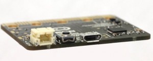
BBC Micro:bit side-on

BBC Micro:bit side-on

The sky’s the limit really. We’ve seen and heard about all sorts of applications already. At the launch event alone there was a Flappy Bird-esque game you could remote control using the Micro:bit buttons. Micro:bits were also being used to trigger the taking of selfies with a smartphone, a remote control truck was being controlled using the Micro:bit accelerometer and apparently one enterprising and creative young developer put together ‘the story of pizza’ using the LED display!

Q: How is a profile actually expressed, if I wanted to create my own custom profile? Is it via XML?

A: If you use Bluetooth Developer Studio you work with an intuitive drag and drop GUI. Behind the scenes we use XML to represent the profile and its constituent parts – the services, characteristics and descriptors. When you generate code that will implement your profile on a particular target platform, you’re generating source code for a particular SDK and each SDK represents a profile in its own way. Some use XML, some use JSON and some require you to build an in-memory description of the profile at run-time by making calls to library functions from your firmware.

Bluetooth Developer Studio goes a long way to protecting you from these variations since you’re working in a platform agnostic way during the design phase and the code generation process takes care of platform variations for you.

Q: Where and how does this get built or compiled?

A: After generating source code from Bluetooth Developer Studio you switch into the native tool chain for the target platform. Doing this is often as simple as double clicking on one of the generated files and watching as the appropriate development tool launches and imports the generated code. It’s here that you make any final, manual adjustments to the code and then build it and flash it to your device.

Once it’s been flashed you can then return to Bluetooth Developer Studio and use the testing workbench to run test scripts against your device, communicating with it using Bluetooth Smart via a dongle plugged into your PC.

Q: Can we all view this Micro Bit profile? Is it publicly documented in any way – alongside the Current Time Service or Blood Pressure Service, for example?

A: It’s not available externally at the moment. We are in discussions with the BBC and the details with other resources relating to the Micro:bit may be released when the time comes.

The future

Q: Getting back to the Micro Bit specifically, what do you feel it brings to the party that wasn’t there before, with the Raspberry Pi or LittleBits or SAM Blocks, for example?

A: The BBC Micro:bit will complement other devices like the wonderful Raspberry Pi (I have two!) and the SIG is sure we’ll see some fantastic creations involving both devices working together coming out of classrooms. The Raspberry Pi is a full blown Linux computer with a traditional screen, keyboard and mouse whereas the Micro:bit is a simpler device with its LED grid and two buttons.

We’ll have to see how kids respond to the Micro:bit and the various tools being created for it but the expectation the BBC has is that the Micro:bit will make it easy for kids to produce exciting and educational results very quickly. It’s also wearable and very small so there are bound to be some great ideas that take advantage of these aspects. With its motion detector and Bluetooth Smart profile, never again will big brother/sister be able to sneak into a younger, Micro:bit owning sibling’s bedroom undetected again!

Q: Any prediction on how it will fare? Or even what sort of apps will emerge, any particular trends?

A: The SIG is hoping that this will be a huge success – the sort of apps that emerge is limited only by the imagination of the kids in the country’s classrooms. The main trend that we’re wanting to see emerge is the growth of a new generation of digital pioneers who will one day take the IoT into exciting new directions. It may be a few years before this is proven true!

Q: Thank you for your time. Let’s hope the project gets the success it deserves – a lot of people have put a lot of effort into it, I know. One to tell the grand-kids about, that you were involved?

A: I’m not quite ready for grand-kids yet – let’s not give my kids ideas, if you don’t mind! But yes, we hope this will be something to look back fondly upon and more importantly, something which energises Britain’s development of the country’s Internet of Things economy.


Alun Williams

Comment: Can Germany keep Europe in the FD-SOI game?

German chancellor Angela Merkel on a visit to Infineon's Dresden fab

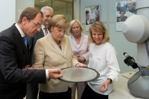
German chancellor Angela Merkel on a visit to Infineon’s Dresden fab

With FD-SOI now being proposed as the next generation semiconductor process technology, the epicentre for semiconductor manufacturing in Europe is shifting to Germany.

With the eclipse of both STMicroelectronics and NXP as major European manufacturers of chips, the new momentum for investment in wafer fabs seems to be coming from Germany alone.

That is if we class Imec in Belgium and France’s CEA-Leti as advanced semiconductor research facilities rather than commercial IC production wafer fabs.

In the past five years, Infineon has invested around €600m in its Dresden fab.

This month international chip foundry Globalfoundries extravagantly heralded the opening of “a new chapter in the Silicon Saxony story, building on almost 20 years of sustained investment in Europe’s largest semiconductor fab”.

The reason for this was a $250m investment in its fab in Dresden for development and initial production of its 22nm FD-SOI (full-depleted silicon-on-insulator) process technology platform called 22FDX.

This is significant because FD-SOI is now being proposed as the next generation semiconductor process technology which, like the finfet alternative being championed by Intel, is expected to drive chips to sub-10nm geometries.

Some observers believe that within five years volume digital chip production will be a square contest between finfet fabs and FD-SOI fabs.

Intel, Samsung and TSMC will be main protagonists with their wafer fabs in the US and Asia.

Globalfoundries is vying to be a prat of that fight. Its main fabs are in the US, courtesy of the IBM fab acquisition.

However, Globalfoundries alone of the big four chip manufacturers does not seem to have given up on Europe. As its continuing investment in FD-SOI capacity in Dresden demonstrates.

Globalfoundries has invested more than $5bn in the Dresden fab since 2009.

This would seem to make the European Commission’s grandiose but somehow directionless plans to create a European wafer fab irrelevant. NXP and ST do not seem than keen on the idea.

NXP is looking global with its acquisition of Freescale and ST has more pressing concerns at home.

So the EC’s only credible option seems to be to channel any chip investment it is prepared to make into the fabs in Dresden, Germany. This would seem unlikely.

So if Europe is to have the wherewithal to make sub-14nm FD-SOI chips in the future it looks like being in Germany, and largely thanks to the commitment of an international foundry, which unlike most other chips firms has not given up on making advanced chips in Europe.


Richard Wilson

UltraSoC joins with Tortuga Pacific to push IP

UltraSoC, the debug specialist, has joined with Tortuga Pacific, the specialist in expanding IP businesses, to promote  UltraSoC’s UltraDebug debug and validation technologies to SoC designers.

Rupert Baines

Rupert Baines

“The Tortuga Pacific team is uniquely equipped to represent UltraSoC’s silicon debug and analytics offering to our key markets in North America, Japan and elsewhere,” says UltraSoC CEO Rupert Baines, “they bring us impeccable sales, business development and strategic credentials, allied with an intimate knowledge of the semiconductor IP space, gained in leadership positions in companies such as GLOBALFOUNDRIES, MIPS Technologies, Si2, Tessera, TI and Xilinx. If I’d set out to design an organization from the ground up to represent UltraSoC, I couldn’t have come up with a better firm than Tortuga.”

SoC debug and silicon validation are key challenges facing the global electronics industry today. UltraSoC’s technology creates an on-chip debug infrastructure that enables pre- and post-silicon debug, de-risking the process of chip design, improving time-to-market, increasing quality and reducing costs.

Chip designers can use UltraSoC technology to “look inside” their products while they operate, and analyze the complex interactions between the different IP building blocks that are commonly used to construct such devices. The features and performance of a chip can be monitored and refined, even after the device has been built into an end product – a particularly powerful capability for connected devices.

“UltraSoC is one of the most exciting companies in the silicon IP space today, with the potential to revolutionize not only SoC development, but also the industry’s fundamental approach to product design,” says  Tortuga’s Brad Holtzinger “debug has traditionally been seen as a cost – an overhead – in the embedded design process. UltraSoC builds analytics and forensics into SoCs, enabling superior end products and turning that cost into a value.”

Read more UltraSoc stories on Electronics Weekly »


david manners

ADI integrates 24-bit sigma-delta converters into sensor interface chip

ADI integrates 24-bit sigma-delta converters into sensor interface chip

ADI integrates 24-bit sigma-delta converters into sensor interface chip

Analog Devices has integrated 24-bit sigma-delta converters into analogue front end devices with up to eight differential inputs.

The AD7124-4 and AD7124-8 are integrated signal chain devices with a programmable gain amplifier, precision reference, reference buffers, current sources, temperature sensor and excitation sources all on-chip.

The AD7124-4 has four differential and seven pseudo-differential inputs and the AD7124-8 has eight differential and 15 pseudo-differential inputs.

The AFEs are designed to be used with devices with analogue outputs such as resistance temperature detectors, thermocouples, voltage/current inputs and current bridges.

The devices offer three user-selectable power modes. In the lowest power mode (255 µA) the converter delivers 21.7 noise free bits at low sampling rates.

The user-selectable power modes allow designers of programmable-logic controllers, process controllers, transmission systems and other industrial and instrumentation equipment to develop a single platform by precisely matching power/performance requirements for each use case.

Features

  • Three power modes
  • RMS noise
  • Up to 22 noise free bits in all power modes (gain = 1)
  • Output data rate
  • Rail-to-rail analog inputs for gains > 1
  • Simultaneous 50 Hz/60 Hz rejection at 25 SPS (single cycle settling)
  • Diagnostic functions (which aid safe integrity level (SIL) certification
  • Crosspoint multiplexed analog inputs
  • 4 differential/7 pseudo differential inputs
  • Programmable gain (1 to 128)
  • Band gap reference with 15 ppm/°C drift maximum (65 μA)
  • Matched programmable excitation currents
  • Internal clock oscillator

Analog Devices writes:

The AD7124-4 is a low power, low noise, completely integrated analog front end for high precision measurement applications. The device contains a low noise, 24-bit Σ-Δ analog-to-digital converter (ADC), and can be configured to have 4 differential inputs or 7 single-ended or pseudo differential inputs. The onchip low gain stage ensures that signals of small amplitude can be interfaced directly to the ADC.

One of the major advantages of the AD7124-4 is that it gives the user the flexibility to employ one of three integrated power modes. The current consumption, range of output data rates, and rms noise can be tailored with the power mode selected. The device also offers a multitude of filter options, ensuring that the user has the highest degree of flexibility.


Richard Wilson

Teachers get free Raspberry Pi skills in Google Digital Garage

Martin O’Hanlon will be leading teachers in Google Digital Garage

Martin O’Hanlon will be leading teachers in Google Digital Garage

Educating students of all ages in embedded design continues to be an important part of the activities of the Raspberry Pi Foundation.

Its programme of training teachers in embedded design based on Raspberry Pi is continuing apace with the numbers of Raspberry Pi-certified educators growing through its training events called Picademies.

It has set up five regional Picademies in the UK and with the support of Google a new Picademy in Birmingham.

Dubbed the Google Digital Garage, the Birmingham centre will be used by classroom teachers of any subject at primary, secondary or post-16 level.

The courses and workshops at the original Picademy in Leeds are run by renowned community member Les Pounder, who gives much of his time to helping adults and children create weird and wonderful projects.

At the Picademy@Google in Birmingham, Raspberry Pi community member and Minecraft wizard Martin O’Hanlon will be leading teachers in the the Raspberry Pi Foundation’s free CPD course.

The opening of the Google Digital Garage at the Library of Birmingham was attended by Eileen Naughton, MD of Google UK and Ireland, and Sajid Javid, Secretary of State for Business, Innovation and Skills.

All training events in Birmingham are free to attend and the following dates are available:

  • 27th – 28th August
  • 1st – 2nd October
  • 2nd – 3rd November
  • 7th – 8th December

Richard Wilson