Server power measured per programme by Fujitsu

Server power measured per programme by Fujitsu

Server power measured per programme by Fujitsu

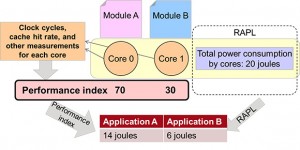
Aiming to cut power waste in data centres, Fujitsu Labs has developed a way to determine how much energy each programme running on a CPU consumes.

It adds to the capability, called RAPL, of some Intel CPUs to measure overall power consumption.

“According to a report by the Japanese Ministry of Internal Affairs and Communications, Japan’s datacenters consume an average of 7.72 billion kWh per year,” said Fujitsu.

“One way to reduce energy consumption is through the use of more energy-efficient hardware. Another is to reduce the energy required to run programs on servers. A precondition for energy-efficient programming is to have an understanding of the energy being consumed by existing software. Until now, however, it was not possible to calculate the energy required to execute software on a core-by-core basis, so it has been difficult to take a software-based approach to reducing power consumption.”

Not a lot of detail has been revealed – it is to be presented at the Summer United Workshops on Parallel, Distributed and Cooperative Processing 2015 (SWoPP 2015) next week.

The Lab’s technique uses information that can be tracked at the individual core level such as clock cycles and cache-hit percentages to estimate energy consumption in detail, down to the program module level. It adds atound 1% processing over-head, and captures information by the millisecond.

Testing is underway, a practical implementation is expected in 2016, and the company is also looking into applying the technology to its own data centres.


steve bush

Server power measured per programme by Fujitsu

Server power measured per programme by Fujitsu

Server power measured per programme by Fujitsu

Aiming to cut power waste in data centres, Fujitsu Labs has developed a way to determine how much energy each programme running on a CPU consumes.

It adds to the capability, called RAPL, of some Intel CPUs to measure overall power consumption.

“According to a report by the Japanese Ministry of Internal Affairs and Communications, Japan’s datacenters consume an average of 7.72 billion kWh per year,” said Fujitsu.

“One way to reduce energy consumption is through the use of more energy-efficient hardware. Another is to reduce the energy required to run programs on servers. A precondition for energy-efficient programming is to have an understanding of the energy being consumed by existing software. Until now, however, it was not possible to calculate the energy required to execute software on a core-by-core basis, so it has been difficult to take a software-based approach to reducing power consumption.”

Not a lot of detail has been revealed – it is to be presented at the Summer United Workshops on Parallel, Distributed and Cooperative Processing 2015 (SWoPP 2015) next week.

The Lab’s technique uses information that can be tracked at the individual core level such as clock cycles and cache-hit percentages to estimate energy consumption in detail, down to the program module level. It adds atound 1% processing over-head, and captures information by the millisecond.

Testing is underway, a practical implementation is expected in 2016, and the company is also looking into applying the technology to its own data centres.


steve bush

IQE joins Obama initiative

drewnelson

Drew Nelson

obama

President Obama and Vice President Biden

IQE has been announced as a key partner in a new consortium to establish the United States’ first Integrated Photonics Institute for Manufacturing Innovation (IP-IMI).

Created as part of President Obama’s National Network for Manufacturing Innovation (NNMI), the IP-IMI was launched this week in Rochester, NY by US Vice President Biden as the sixth of nine new manufacturing institutes designed to bring industry together with academia and government to advance the state-of-the-art in the design, manufacture, testing, assembly, and packaging of photonic integrated circuits and establish US Leadership in Integrated Photonics.

“IQE is proud to have been named as one of 55 key industrial partners in this important project led by SUNY to accelerate photonic capabilities and manufacturing in the U.S,” says IQE CEO Dr Drew Nelson, “the importance of the rapidly growing photonics technology industry cannot be overestimated and is already having a major impact in areas such as communications, energy efficiency, healthcare and safety and security systems. Inclusion as a key partner in this new US Manufacturing Institute is testament to IQE’s reputation as a global world leader in compound semiconductor materials, a key enabling technology (KET) for photonics.”

The consortium comprises 55 leading industrial partners, including Intel, IBM, Infinera, HP, Honeywell, Rockwell, Seagate and TI along with numerous other leading edge companies, universities and laboratories, and is led by the Research Foundation of the State University of New York (SUNY). IQE’s role in the consortium is to provide advanced epitaxy services to the Institute partners.

The IP-IMI has been awarded federal funding of $110 million by the Department of Defense, which is expected to yield total public-private investment of more than $610 million which will enable the institute to focus on developing an end-to-end integrated photonics ecosystem in the U.S., including domestic foundry access, integrated design tools, automated packaging, assembly and test, and workforce development. The Institute will develop and demonstrate innovative manufacturing technologies for:

  • Ultra-high-speed transmission of signals for the internet and telecommunications
  • New high-performance information-processing systems and computing
  • Compact sensor applications enabling dramatic medical advances in diagnostics and treatment
  • Multi-sensor applications including urban navigation, free space optical communications and quantum information sciences
  • Other diverse military applications including electronic warfare, analog RF sensing, communications, and chemical/biological detection
  • All of these developments will require cross-cutting disciplines of design, manufacturing, packaging, reliability and testing.
  • Photonics is widely recognised globally as a key enabling technology that has significant potential to revolutionize a wide range of commercial, industrial and defense applications, including:
  • Revolutionizing communications
  • Creating dramatic energy savings at high-performing data centres
  • Dramatically improving medical technologies
  • Improving safety and security operations

The institute will provide central facilities through which academia, SMEs and large corporations can access latest technology for design and manufacture of photonics devices providing a route to commercialisation through high-value, high-volume manufacturing.

More IQE stories on Electronics Weekly »

david manners

Infineon on-track to 34% y-o-y growth

Infineon had calendar Q2 revenue of € 1,586 million – up 7% on calendar Q1 – for a profit of €245 million at a margin of 15.4%. Infineon expects a 1% revenue increase in calendar Q3 and a 34% increase for the full year.

Dr Reinhard Ploss, Infineon

Dr Reinhard Ploss, Infineon

“Revenue, earnings and margin rose significantly in the quarter, despite an increasingly difficult business environment,” says Infineon CEO Reinhard Ploss, “for the full fiscal year, we therefore continue to forecast revenue and a Segment Result Margin within the ranges previously predicted. The integration of International Rectifier is progressing according to plan.”

Between its four main operating units, revenues split: Automotive €621 million, Industrial Power Management €269 million, Power Management and Multimarket €517 million and ChipCard and Security €172 million.

Overall group operating income improved from €79 million in calendar Q1 to €119 million in calendar Q2 while net income for calendar Q2 came in at €109 million, well ahead of the previous quarter’s €65 million.

Payment of the purchase price for International Rectifier had given rise to a negative Free Cash Flow of €1,880 million in calendar Q1.

Net cash provided by operating activities from continuing operations rose from €135 million to €432 million. The gross cash position went up from €1,656 million on March 31, 2015 to €1,842 million at the end of calendar Q2.

The net cash position improved over the same period from a negative amount of €176 million to stand at a positive amount of €49 million at June 30, 2015.
With these figures, Infineon is now back within the target range for its three capital management objectives, namely gross cash of between 30 and 40% of revenue, a positive net cash position, and a moderate level of debt.

All four operating segments will contribute to revenue growth in 2015.

Investments during the 2015 fiscal year are expected to be in the region of €800 million. This figure includes investments in plant and equipment at existing factories and in intangible assets including capitalized development costs.

Specifically included in these investments are €60 to €70 million for readying the second shell in Kulim, Malaysia, for volume production and €21 million for the purchase of Qimonda patents in conjunction with the settlement reached with the insolvency administrator of Qimonda AG.

Depreciation and amortization will increase to around €750 million, mostly as a result of acquisition-related charges.

Read more Infineon stories on Electronics Weekly »


david manners

Toshiba licenses ARM Cortex-A53

ARM Cortex A53 chip diagram

ARM Cortex A53, based on ARMv8-A

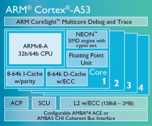
Toshiba has licensed the ARM Cortex-A53 processor, the most power-efficient ARMv8-A processor capable of seamlessly supporting 32-bit and 64-bit code.

Toshiba will deploy the processor to develop ASSPs such as ApP LiteT application processors that offer well balanced power-efficiency and performance with 64-bit capability, and custom products such as FFSA (Fit Fast Structured Array) and ASIC for industrial, networking, IoT, automotive and data storage products.

The Company expects to bring products to market at an early date, it says.

The industrial market is seeing strong demand for 64-bit capabilities and high reliability. The network market requires high-speed, low-power-consumption operation, real time processing and multi-clustered storage systems for huge data handling and data encryption. IoT products require power-efficient microprocessors, and applications relying on enormous storage capacity need an expanded memory address space. Toshiba will develop products to meet these various demands.

According to the company, the processor will allow Toshiba to hasten the development of highly featured, high performance systems that meet the functional safety requirements of ISO26262 for the automotive market and to provide customers with solutions for next generation automotive applications.

The Cortex-A53 processor features an 8-stage in-order pipeline, and strengthened data access / instruction fetch techniques. It also features ARM NEON technology with enhanced multimedia handling capabilities in addition to 128-bit SIMD ordering capabilities, as well as a cryptographic engine that accelerates encryption handling such as AES (Advanced Encryption Standard) and SHA (Secure Hash Algorithm) by extending architectures.

“Toshiba’s commitment to build SoCs based on Cortex-A53 further highlights the diverse range of use cases for the industry’s leading low-power 64-bit processor,” said Nandan Nayampally, vice president, marketing, CPU group, ARM. “The Cortex-A53 will deliver new levels of compute performance into power and space constrained environments in automotive, IoT and networking infrastructure applications and the processor safety package enables Toshiba to create products compliant with the latest functional safety standards.”


david manners

In depth: NASA’s passive Wi-Fi saves 80% power

NASA passive WiFi chip NASA has revealed a technique which dramatically cuts the power consumption of Wi-Fi comms, at least at the remote terminal.

Key is modifying the Wi-Fi base station to allow the transmitter of the remote terminal to be replaced by a modulated passive reflector.

“In a Wi-Fi radio, 70-80% of power is consumed generating Wi-Fi signal. If you only reflect, you save the transmit power,” Adrian Tang of NASA’s Jet Propulsion Laboratory told Electronics Weekly. Tang is working with Frank Chang at UCLA.

What returns to the basestation is not some pale shadow of Wi-Fi.

“You get PHY, header, and everything; you get real Wi-Fi comms back,” said Tang.

The scheme works like this:

The basestation is modified to emit a 20dBm continuous-wave (CW) sinewave at the Wi-Fi fundamental frequency, while the remote terminal has an antenna connected to a variable phase shifter and a load.

Even without the phase shifter, the remote terminal can amplitude-modulate reflected signals by switching the load between matched and short-circuit.

With the right phase shift options, the signal reflected back from the antenna can be a clean Wi-FI signal with modulation up to 16-QAM – and phase shifters can be as simple as switches connecting the antenna to transmission lines of various lengths.

Tang and Chang have implemented such a modulator, offering QPSK and ASK as well as covering 2.4 or 5.83GHz, on a CMOS chip – its 200µm2 footprint is small enough to be added to a baseband SoC.

“At the remote terminal, there is no synthesiser, no power amplifier, just a modulator; and the modulator is just a bunch of switches,” said Tang.

For the demonstrator, the chip also includes a pseudo-random number generator.

The basestation has a conventional Wi-Fi receiver chip, but it needs some help as its receive antenna gets the smaller-than-usual modulated signal, swamped by reflections of the original CW transmission from the local environment. The CW reflections add-up to a single CW signal of arbitrary phase and amplitude, and put reception well outside the dynamic range of conventional Wi-Fi chip front-ends.

To get over this, Tang and Chang have created a second chip (see photo) which sits between the basestation receive antenna and the conventional Wi-Fi chip.

The second chip, made in 65nm CMOS, takes a sample of the transmitted CW signal and, via a variable phase shifter and a variable attenuator (right in the photo), adds it to the received signal.

With the correct phase shift and attenuation, most of the incoming CW signal can be nulled, leaving the Wi-Fi signal. Feedback loops in the on-chip signal processor updates phase and amplitude settings every 100µs.

“We can get about 60dB of suppression. We don’t actually need it all. We only need to stop the receiver from compressing,” said Tang. “10-20dB is good enough for a normal Wi-Fi chip.”
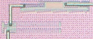
NASA passive WiFi chip phase amplitudeNASA passive WiFi chip antenna interfaceIn the photos, the central block is the signal processor. The right-hand circuit samples the CW transmit signal. Its two horizontal structures are a variable phase shifter above a variable attenuator.
On the left hand side is the antenna interface circuit.

So far, the scheme has been tested at up to 6m, with 330Mbit/s achieved at 2.5m range.

One fly-in-the-ointment is that Wi-Fi basestations are not permitted to transmit CW signals.

“We are working to make it 100% Wi-Fi standard compatible,” said Tang.

Patents have been applied for and applications in wearables where battery life is important are expected , said NASA, adding: “There are agreements in place for the commercialisation of the technology.”

The idea behind the scheme came out of a NASA project to eliminate mechanically-steered antennas in space – whose pivots have a habit of seizing, according to Tang.

Conventionally, the mechanically-fixed alternative is beam-forming using a fixed planar array of antennas, each driven by a separately phase-shifted signal through its own power amplifier, or low-noise amplifier (LNA) in the receive case.

NASA instead is experimenting with a single power amplifier and fixed antenna, bouncing its energy off a fixed planar array of reflective antennas, each with its own variable phase-shifter to steer the beam. If it works, it will remove the need for multiple power amplifiers or LNAs.

steve bush