The internet of things relies on getting good quality sensor data at the right time in the right format, which is why energy harvesting wireless sensors are of special interest, writes Matthias Kassner

In the Sauter ecoUnit wireless room operating unit, a temperature sensor powered by a solar cell has enabled increased comfort with significantly reduced energy consumption
Energy harvesting wireless sensors have sparked a dramatic rise in interest, since they represent a reliable and easy‑to‑install technology that delivers the essential input data on which the whole internet of things (IoT) model depends. Creating a sensor node that handles the essential data capture, processing and transmission with the minimal energy that can be harvested from the environment is a challenge.
There are three key tasks in energy harvesting wireless sensors: generating (harvesting) the required energy, sensing and processing environmental parameters (temperature, humidity, position) and wirelessly transmitting the collected information. All three tasks need to be optimised together to provide viable solutions.
Energy-efficient system design
The most common forms of energy harvested by IoT sensors are kinetic, solar and thermal (see box, opposite).
All three harvesting technologies provide comparatively small amounts of energy (typically in the microampere range). Power-optimised system design is therefore essential to enable wireless sensors based on these energy sources.
Three main tasks define the power budget of a wireless sensor node – sensor measurement, wireless transmission and idle (inactive) state. System design must balance the harvested energy with the power requirements of these tasks.
This balance can be established in two directions – either the system functionality (and hence the required power) is fixed and the harvester is scaled, or the energy delivery of the harvester is fixed and the system functionality needs to be optimised. The second case is the more common one.

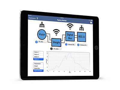
The functionality described in this article has been implemented in the EnOcean STM 330 energy harvesting temperature sensor which can be extended with the HSM 100 humidity sensor
To illustrate the requirements, consider the case of a solar-based room control unit. Its main tasks are to measure temperature and humidity in a room and compare them with user-defined set points (usually target temperature only, sometimes also target humidity).
The available energy budget is limited by the available size for the solar cell (say 5cm2) and the expected minimum illumination level (200Lux for six hours).
Considering the typical performance of standard indoor solar cells, this means that we need to design the sensor system to consume less than 1µA average current.
For simplicity’s sake we will subsequently calculate based on average current under the assumption that the supply voltage is fixed to 3V. To assess the functionality boundaries, we will initially allocate the available energy equally over the three main tasks giving about 300nA of average current each for sensing, wireless transmission and sleep/power loss.
An optimised temperature and humidity sensing implementation would require the equivalent of approximately 1mA current for a period of 10ms for sensor operation, data exchange between sensor and processor (via I2C or a similar bus) and initial data processing. We can then calculate the maximum number of measurements per day by comparing the available energy per day (300nA x 86.4s) with the required energy per measurement (1mA x 10ms) and find that the initial energy budget would allow for 2,592 measurements per day.
Considering that temperature and humidity change only slowly and that we need to conserve energy, we set a rate of one measurement per minute (1,440 per day).
Moving to the radio transmission, we assume an average current of 25mA for formatting and transmission of data at a rate of 125kbit/s. Based on the available power budget and the required transmission current we calculate the total possible transmission time per day which equals just over one second (or 125,000 bits/15,625 bytes) per day.
Putting this in relation to the possible number of measurements, we can identify a key constraint of energy harvesting wireless sensors – the radio protocol must be optimised for minimum size. We would need to limit the total telegram length to 10 bytes in order to transmit each measurement result in one radio telegram.
From this, it is clear that both the radio protocol and the amount of transmission need to be optimised.
Energy-optimised protocols
The payload associated with sensors is often small (a few bytes), therefore an optimised protocol must limit the transmission overhead (frame control, preamble, synchronisation, error checking) as much as possible while maintaining highly reliable communication.
Standard IP protocol (UDP over IPv6) requires more than 50 bytes of overhead; therefore native IPv6 communication is usually not possible in energy harvesting sensor applications. The power optimised ISO/IEC 14543-3-1X protocol, in contrast, requires only 12 bytes in total for the transmission of 1 byte of sensor data. Using such protocol in conjunction with an intelligent transmission strategy (transmission of significant changes only) enables even use of redundant sub-telegrams to increase transmission reliability.
Minimising sleep losses
Energy harvesting wireless sensors must be in an ultra-low power sleep state for more than 99.99% of the time. Minimising power consumption in this state is therefore absolutely essential.
Considering our design example, we have a total budget of 300nA which needs to cover processor consumption in sleep mode (with the ability for timer-based periodic wake-up) as well as losses due to leakage in the energy store.
Such a low level of power consumption is difficult to achieve, even with the latest processors, and is probably the biggest design challenge. Custom mixed-signal designs and optimised system architecture are required to address these challenges.
From wired proximity to wireless
Today, input data for the IoT is often provided by wired sensors that are locally connected to controllers and actuators.
Here, all network components are in close proximity and directly connected with each other.
This approach is well suited to local applications with limited flexibility needs where data reuse is not required.
The internet of things, in contrast, no longer requires such proximity. It allows centralised or even cloud-based data processing.
Thus, the same data can be used for several applications, driving down infrastructure cost and allowing dynamic network structures.
All of these characteristics require a second cloud, consisting of sensor and actuator nodes that can be deployed and expanded flexibly.
Nodes that use minimal energy, which they harvest from their surroundings, provide a fit-and-forget solution – they can be installed in the most inaccessible locations and relied upon to execute their task with minimal maintenance or attention.
Technologies for harvesting energy
Energy can be harvested from different sources; the most commonly used are:
- Kinetic energy – Kinetic energy in different forms (lateral movement, rotation or vibration) has long been used to generate electrical energy using electromagnetic or piezoelectric harvesters. For most applications, the electromagnetic energy harvester is the better choice as it provides a more stable energy output at a longer life cycle without ageing effects. These harvesters generally work by changing the magnetic flux through a coil either by moving a magnet relative to the coil or by changing the flux polarity. This type of kinetic energy harvesting is the technology of choice for mechanical switches and similar applications.
- Solar energy – Many sensor applications are powered by miniaturised solar cells. They are well suited for applications with sufficient illumination (indoor or outdoor) and often used for sensor applications such as temperature, humidity, illumination or CO2 sensors. Energy delivery can be scaled by adjusting the size of the solar cell based on the available space set by the application.
- Thermal energy – Temperature differences can be used to generate energy based on Peltier elements. The standard application for these elements is to cool an area (such as a cooling box) when electrical energy is applied. The reverse effect – generating energy based on temperature differences – is used for thermal harvesting. The output voltage of Peltier elements depends on the temperature difference and is typically very small (20mV for °C temperature difference). Specialised electronics is therefore required to utilise this energy.
Matthias Kassner is product marketing director at EnOcean