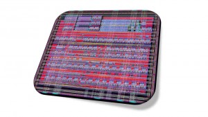
Stanene: two-dimensional tin

Two dimensional tin has been fabricated by a Chinese-American team. It is potentially a large band-gap semiconductor with unusual properties that include topological superconductivity and near-room-temperature quantum anomalous Hall effect, according to the Nature Materials paper ‘Epitaxial growth of two-dimensional stanene‘.

Topological superconductivity is the free conduction of electrons along the outside edges of a two dimensional material.

Stanene now joins 2D silicon (silicene) and 2D germanium (germanene) from group IV of the periodic table.

The team found a suitable hexagonal crystal to grow it on – (111) Be2Te3 – and deposited it using molecular beam epitaxy – MBE was how other teams managed to fabricates silicene and germanene, and germanene has also been made by mechanical exfoliation.

What grows is not totally flat like graphene, but a molecule with a regular slight buckle – every second atom is either slightly up or slightly down from the molecular plane – resembling two layers when viewed from the side. The height difference is around 0.1nm.

This is early days for the material, which interacted with the substrate and could not be measured in isolation. Work with the bare substrate, the substrate plus stanene, and then further over-coated with potassium, allowed theoretical models to be confirmed and improved. “The synthesis of stanene and its derivatives will stimulate further experimental investigation of their theoretically predicted properties”, said researchers in the paper’s abstract.

Scientists took part from: Shanghai Jiao Tong University, Stanford University, Tsinghua University, Collaborative Innovation Center of Quantum Matter (Beijing) and Collaborative Innovation Center of Advanced Microstructures (Nanjing).


steve bush

NTT Docomo taps up Intel for 5G research

video_call_w100Japanese mobile operator NTT Docomo is to work with Intel and Qualcomm as part of its development of 5G research into mobile communications technologies.

NTT Docomo has also signed up Panasonic and Rohde & Schwarz as part of the ongoing development of 5G mobile communications.

Last month, Keysight Technologies also said is was to work with Japan’s main mobile operator on 5G communication system development.

Like other mobile operators, NTT Docomo is working toward a commercial launch of 5G services in 2020. The goal is to provide an initial 5G deployment in time for the Tokyo 2020 Olympic Games.

But 5G technology development is still in its early stages.

Docomo has been working with Alcatel-Lucent, Ericsson, Fujitsu, Huawei, Mitsubishi Electric, NEC, Nokia and Samsung on 5G research for just over a year.

The first 5G standards are not expected to be confirmed before next year. Current work is focusing on the radio interface and the frequency band with the capacity to support the scale of data traffic 5G will bring.

NTT Docomo writes in a white paper on 5G technology development:

“5G, compared to 4G, needs to be more massive and scalable to enable a wider range of scenarios and services. In particular, the 5G radio access needs to provide significant performance gains in system capacity and user data rates. Specifically, it is necessary to meet the very challenging  targets of 1000-fold system capacity per km and Gbit/s-order user-experienced data rate. This  necessitates the pursuit of not a single but a set of directions of evolution for radio access  technologies.”

NTT Docomo proposes two basic evolution paths that can be taken to support new system capabilities for 5G:

1) An evolutionary path focusing on further LTE enhancements.

2) A revolutionary path using a brand-new radio access technology that may include major changes that are non-backward compatible with LTE.

Docomo believes that LTE/LTE-Advanced, well-optimised for existing lower frequency bands, will continue  to be improved in the future.

“LTE/LTE-Advanced  could even be further enhanced to cover some of the 5G system capabilities, such as massive  connectivity and reduced latency. However, the challenges of achieving significant gains in capacity and user-experienced data rate will require a significant leap in spectrum efficiency, spectrum extension, and network densification and LTE/LTE-Advanced and their enhancements alone are unlikely to accomplish,” says the NTT Docomo white paper.

“From spectrum utilization point of view, the spectrum below 3GHz is mostly utilised by existing systems. The utilization of higher frequency bands will enable higher data rates (maybe also lower latency) by using wider bandwidths. For higher frequency bands, e.g., beyond 10GHz, the current 4G system (LTE/LTE-Advanced radio interface) would not be an optimum  solution because it has been optimised for the existing cellular bands, i.e., around 2GHz.

“Thus, the use of higher frequency bands requires a new radio access technology and therefore, Docomo considers 5G radio access as a combination of a new radio access technology specifically designed for higher frequency bands and LTE/LTE-Advanced enhancements.”

Lower power millimetre wave transmission in the 60GHz band is being considered for 5G because of the scarcity of spectrum resources below 6GHz, which leads to high interference levels, the public concern about microwave electromagnetic field (EMF) exposure in dense areas and the power consumption of the infrastructure.

Rohde & Schwarz has the SMW200A vector signal generator and the FSW85 spectrum analyser which cover the frequency range up to 85GHz in a single sweep without the need of external harmonic mixers. This is suitable for measurements in the millimeter-wave frequency band being investigated for 5G development.

Rohde & Schwarz is already a partner in the UK’s main 5G technology development project at the 5GIC on the University of Surrey campus.


Richard Wilson

NTT Docomo taps up Intel for 5G research

video_call_w100Japanese mobile operator NTT Docomo is to work with Intel and Qualcomm as part of its development of 5G mobile communications technologies.

NTT Docomo has also signed up Panasonic and Rohde & Schwarz as part of the ongoing development of 5G mobile communications.

Last month, Keysight Technologies also said is was to work with Japan’s main mobile operator on 5G communication system development.

Like other mobile operators, NTT Docomo is working toward a commercial launch of 5G services in 2020. The goal is to provide an initial 5G deployment in time for the Tokyo 2020 Olympic Games.

But 5G technology development is still in its early stages.

Docomo has been working with Alcatel-Lucent, Ericsson, Fujitsu, Huawei, Mitsubishi Electric, NEC, Nokia and Samsung on 5G research for just over a year.

The first 5G standards are not expected to be confirmed before next year. Current work is focusing on the radio interface and the frequency band with the capacity to support the scale of data traffic 5G will bring.

NTT Docomo writes in a white paper on 5G technology development:

“5G, compared to 4G, needs to be more massive and scalable to enable a wider range of scenarios and services. In particular, the 5G radio access needs to provide significant performance gains in system capacity and user data rates. Specifically, it is necessary to meet the very challenging  targets of 1000-fold system capacity per km and Gbit/s-order user-experienced data rate. This  necessitates the pursuit of not a single but a set of directions of evolution for radio access  technologies.”

NTT Docomo proposes two basic evolution paths that can be taken to support new system capabilities for 5G:

1) An evolutionary path focusing on further LTE enhancements.

2) A revolutionary path using a brand-new radio access technology that may include major changes that are non-backward compatible with LTE.

Docomo believes that LTE/LTE-Advanced, well-optimised for existing lower frequency bands, will continue  to be improved in the future.

“LTE/LTE-Advanced  could even be further enhanced to cover some of the 5G system capabilities, such as massive  connectivity and reduced latency. However, the challenges of achieving significant gains in capacity and user-experienced data rate will require a significant leap in spectrum efficiency, spectrum extension, and network densification and LTE/LTE-Advanced and their enhancements alone are unlikely to accomplish,” says the NTT Docomo white paper.

“From spectrum utilization point of view, the spectrum below 3GHz is mostly utilised by existing systems. The utilization of higher frequency bands will enable higher data rates (maybe also lower latency) by using wider bandwidths. For higher frequency bands, e.g., beyond 10GHz, the current 4G system (LTE/LTE-Advanced radio interface) would not be an optimum  solution because it has been optimised for the existing cellular bands, i.e., around 2GHz.

“Thus, the use of higher frequency bands requires a new radio access technology and therefore, Docomo considers 5G radio access as a combination of a new radio access technology specifically designed for higher frequency bands and LTE/LTE-Advanced enhancements.”

Lower power millimetre wave transmission in the 60GHz band is being considered for 5G because of the scarcity of spectrum resources below 6GHz, which leads to high interference levels, the public concern about microwave electromagnetic field (EMF) exposure in dense areas and the power consumption of the infrastructure.

Rohde & Schwarz has the SMW200A vector signal generator and the FSW85 spectrum analyser which cover the frequency range up to 85GHz in a single sweep without the need of external harmonic mixers. This is suitable for measurements in the millimeter-wave frequency band being investigated for 5G development.

Rohde & Schwarz is already a partner in the UK’s main 5G technology development project at the 5GIC on the University of Surrey campus.


Richard Wilson

NTT Docomo taps up Intel for 5G research

video_call_w100Japanese mobile operator NTT Docomo is to work with Intel and Qualcomm as part of its development of 5G mobile communications technologies.

NTT Docomo has also signed up Panasonic and Rohde & Schwarz as part of the ongoing development of 5G mobile communications.

Last month, Keysight Technologies also said is was to work with Japan’s main mobile operator on 5G communication system development.

Like other mobile operators, NTT Docomo is working toward a commercial launch of 5G services in 2020. The goal is to provide an initial 5G deployment in time for the Tokyo 2020 Olympic Games.

But 5G technology development is still in its early stages.

Docomo has been working with Alcatel-Lucent, Ericsson, Fujitsu, Huawei, Mitsubishi Electric, NEC, Nokia and Samsung on 5G research for just over a year.

The first 5G standards are not expected to be confirmed before next year. Current work is focusing on the radio interface and the frequency band with the capacity to support the scale of data traffic 5G will bring.

NTT Docomo writes in a white paper on 5G technology development:

“5G, compared to 4G, needs to be more massive and scalable to enable a wider range of scenarios and services. In particular, the 5G radio access needs to provide significant performance gains in system capacity and user data rates. Specifically, it is necessary to meet the very challenging  targets of 1000-fold system capacity per km and Gbit/s-order user-experienced data rate. This  necessitates the pursuit of not a single but a set of directions of evolution for radio access  technologies.”

NTT Docomo proposes two basic evolution paths that can be taken to support new system capabilities for 5G:

1) An evolutionary path focusing on further LTE enhancements.

2) A revolutionary path using a brand-new radio access technology that may include major changes that are non-backward compatible with LTE.

Docomo believes that LTE/LTE-Advanced, well-optimised for existing lower frequency bands, will continue  to be improved in the future.

“LTE/LTE-Advanced  could even be further enhanced to cover some of the 5G system capabilities, such as massive  connectivity and reduced latency. However, the challenges of achieving significant gains in capacity and user-experienced data rate will require a significant leap in spectrum efficiency, spectrum extension, and network densification and LTE/LTE-Advanced and their enhancements alone are unlikely to accomplish,” says the NTT Docomo white paper.

“From spectrum utilization point of view, the spectrum below 3GHz is mostly utilised by existing systems. The utilization of higher frequency bands will enable higher data rates (maybe also lower latency) by using wider bandwidths. For higher frequency bands, e.g., beyond 10GHz, the current 4G system (LTE/LTE-Advanced radio interface) would not be an optimum  solution because it has been optimised for the existing cellular bands, i.e., around 2GHz.

“Thus, the use of higher frequency bands requires a new radio access technology and therefore, Docomo considers 5G radio access as a combination of a new radio access technology specifically designed for higher frequency bands and LTE/LTE-Advanced enhancements.”

Lower power millimetre wave transmission in the 60GHz band is being considered for 5G because of the scarcity of spectrum resources below 6GHz, which leads to high interference levels, the public concern about microwave electromagnetic field (EMF) exposure in dense areas and the power consumption of the infrastructure.

Rohde & Schwarz has the SMW200A vector signal generator and the FSW85 spectrum analyser which cover the frequency range up to 85GHz in a single sweep without the need of external harmonic mixers. This is suitable for measurements in the millimeter-wave frequency band being investigated for 5G development.

Rohde & Schwarz is already a partner in the UK’s main 5G technology development project at the 5GIC on the University of Surrey campus.


Richard Wilson
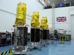
UK-built SSTL satellites will be used for city planning in China

DMC3 satellites

DMC3 satellites

Three Earth observation satellites designed and built by UK-based Surrey Satellite Technology (SSTL) have been placed in a low earth orbit, from where they will provide Earth observation.

The launch of the SSTL satellites is an example of the international nature of space technology in 2015.

The UK-manufactured satellites were launched last month from the Satish Dhawan Space Centre, Sriharikota launch site in India.

This is part of an Anglo-China trade deal. A commercial Earth observation satellite operator based in Beijing, called 21AT, has bought the imaging capacity of the three satellites.

The co-operative contract for the DMC3/TripleSat Constellation was signed in London in 2011 and witnessed by the UK prime minister, and China’s premier.

Monitoring applications include urban planning and management, based on changes detected by the satellite images.

The high resolution imager on board the 450kg SSTL-300S1 series satellites was designed and manufactured by SSTL and will provide 1m ground sampling distance (GSD) in panchromatic mode, and 4m GSD in multispectral mode, with a swath width of 23.4km.

The three satellites will be phased 120 degrees apart around the same orbit using their on board propulsion systems within three months after the launch; thus with off-pointing capability, the satellite constellation will be able to target anywhere on Earth once per day.

According to Sir Martin Sweeting, executive chairman of SSTL, these satellites are “the most advanced of SSTL’s Earth Observation spacecraft mounted on a PSLV rocket dedicated to our mission”.

The next stage is for SSTL’s engineers to commission of the platform systems on board the three satellites, from their Space centre at Guildford, Surrey.


Richard Wilson

UK-built satellites will be used for city planning in China

DMC3 satellites

DMC3 satellites

Three Earth observation satellites designed and built by UK-based Surrey Satellite Technology (SSTL) have been placed in a low earth orbit, from where they will provide Earth observation.

The launch of the SSTL satellites is an example of the international nature of space technology in 2015.

The UK-manufactured satellites were launched last month from the Satish Dhawan Space Centre, Sriharikota launch site in India.

This is part of an Anglo-China trade deal. A commercial Earth observation satellite operator based in Beijing, called 21AT, has bought the imaging capacity of the three satellites.

The co-operative contract for the DMC3/TripleSat Constellation was signed in London in 2011 and witnessed by the UK prime minister, and China’s premier.

Monitoring applications include urban planning and management, based on changes detected by the satellite images.

The high resolution imager on board the 450kg SSTL-300S1 series satellites was designed and manufactured by SSTL and will provide 1m ground sampling distance (GSD) in panchromatic mode, and 4m GSD in multispectral mode, with a swath width of 23.4km.

The three satellites will be phased 120 degrees apart around the same orbit using their on board propulsion systems within three months after the launch; thus with off-pointing capability, the satellite constellation will be able to target anywhere on Earth once per day.

According to Sir Martin Sweeting, executive chairman of SSTL, these satellites are “the most advanced of SSTL’s Earth Observation spacecraft mounted on a PSLV rocket dedicated to our mission”.

The next stage is for SSTL’s engineers to commission of the platform systems on board the three satellites, from their Space centre at Guildford, Surrey.


Richard Wilson

UK built satellites will be used for city planning in China

DMC3 satellites

DMC3 satellites

Three Earth observation satellites designed and built by UK-based Surrey Satellite Technology (SSTL) have been successfully placed in a low earth orbit from where they will provide Earth observation.

The launch of the SSTL satellites is an example of the international nature of space technology in 2015.

The UK manufactured satellites were launched last month from the Satish Dhawan Space Centre, Sriharikota launch site in India.

This is part of an Anglo-China trade deal. A commercial Earth observation satellite operator based in Beijing, called 21AT, has bought the imaging capacity of the three satellites.

The cooperative contract for the DMC3/TripleSat Constellation was signed in London in 2011 and witnessed by the UK Prime Minister, and China’s Premier.

Monitoring applications include urban planning and management, based on changes detected by the satellite images.

The high resolution imager on board the 450kg SSTL-300S1 series satellites was designed and manufactured by SSTL and will provide 1 metre ground sampling distance (GSD) in panchromatic mode, and 4 metre GSD in multispectral mode, with a swath width of 23.4km.

The three satellites will be phased 120 degrees apart around the same orbit using their on board propulsion systems within three months after the launch; thus with off-pointing capability, the DMC3/TripleSat Satellite Constellation will be able to target anywhere on Earth once per day.

According to Sir Martin Sweeting, executive chairman of SSTL, these satellites are “the most advanced of SSTL’s Earth Observation spacecraft mounted on a PSLV rocket dedicated to our mission.”

The next stage is for SSTL’s engineers to commission of the platform systems on board the three satellites, from their Space centre at Guildford, Surrey.


Richard Wilson

IP extracts on-chip performance data on TSMC 28HPC process

moortecDesign reliability for sub-micron chips is highly dependent on physical parameters such as voltage and temperature. UK-based silicon intellectual property (IP) developer Moortec Semiconductor is offering chip designers process, voltage and temperature monitoring and optimisation IP for CMOS geometries such as 40nm, 28nm and FinFET.

The IP embeds monitors within System on Chip (SoC) designs for sensing die temperature, detecting logic speed and monitoring voltage supply levels.

The data can then be used to vary system clock frequencies and the voltage levels of supply domains.

Moortec has created the IP called Embedded Process Detector (MEPD) for the TSMC 28HPC process. It provides the designer with on-chip data which can be used for optimisation of the design, which the Plymouth-based company calls Dynamic Voltage & Frequency Scaling (DVFS).

The embedded IP will detect the process variations brought about by manufacturing variability and drift of advanced node core digital MOS devices.

It is possible to monitor manufacturing variations on and if required, across chip, gate delay measurements, critical path analysis, critical voltage analysis and also monitor silicon ‘ageing’.

The company believes IC designers will increasingly need to analyse this data harvested from in-chip monitors during the life time of every device.

“The greater process variability that is apparent at these challenging small geometry CMOS technologies is forcing the IC design community to look at conditions on-chip, not just generally but also per device and within regions of a device,” said Stephen Crosher, managing director of Moortec Semiconductor.

“At low-geometry nodes, track and via resistances are dramatically increasing, core supply headroom is diminishing and the power consumption per unit area of silicon is increasing, whether that be through static leakage current or dynamic current consumption”

Moortec is looking at monitor on-chip interfaces such as AMBA plans to make the IP available on 28-nm and FinFET process nodes.

Moortec Semiconductor is a 10-year-old Plymouth-based company developing analogue and mixed-signal IP.


Richard Wilson

IP extracts on-chip performance data on TSMC 28HPC process

moortecDesign reliability for sub-micron chips is highly dependent on physical parameters such as voltage and temperature.

UK-based silicon intellectual property (IP) developer Moortec Semiconductor is offering chip designers process, voltage and temperature monitoring and optimisation IP for CMOS geometries such as 40nm, 28nm and FinFET.

The IP embeds monitors within System on Chip (SoC) designs for sensing die temperature, detecting logic speed and monitoring voltage supply levels.

The data can then be used to vary system clock frequencies and the voltage levels of supply domains.

Moortec has created the IP called Embedded Process Detector (MEPD) for the TSMC 28HPC process. It provides the designer with on-chip data which can be used for optimisation of the design, which the Plymouth-based company calls Dynamic Voltage & Frequency Scaling (DVFS).

The embedded IP will detect the process variations brought about by manufacturing variability and drift of advanced node core digital MOS devices.

It is possible to monitor manufacturing variations on and if required, across chip, gate delay measurements, critical path analysis, critical voltage analysis and also monitor silicon ‘ageing’.

The company believes IC designers will increasingly need to analyse this data harvested from in-chip monitors during the life time of every device.

“The greater process variability that is apparent at these challenging small geometry CMOS technologies is forcing the IC design community to look at conditions on-chip, not just generally but also per device and within regions of a device,” said Stephen Crosher, managing director of Moortec Semiconductor.

“At low-geometry nodes, track and via resistances are dramatically increasing, core supply headroom is diminishing and the power consumption per unit area of silicon is increasing, whether that be through static leakage current or dynamic current consumption”

Moortec is looking at monitor on-chip interfaces such as AMBA plans to make the IP available on 28-nm and FinFET process nodes.

Moortec Semiconductor is a 10-year-old Plymouth-based company developing analogue and mixed-signal IP.


Richard Wilson