Ergonomics of Bloodhound

Cambridge Design Partnership Bloodhound

Cambridge Design Partnership Bloodhound

Cambridge Design Partnership has re-worked the design of Bloodhound’s steering wheel.

“The initial steering wheel design was created by the Bloodhound team using a number of novel design techniques including bio-mimicry, crowd sourcing and drawing on experience from Thrust SSC,” said the Parnership.

According to the firm, the original geometry of the grip area was retained from a clay model supplied, while push buttons were relocated.

“The new layout now allows a single fluid rotation movement of the thumb to transition from the power grip used when driving into an activation grip required to press buttons. This revised position could save between 0.5 and 3 football pitches of distance during the deceleration phase of each run,” said the Partnership, adding that it also “incorporated swooping curves across the top and bottom of the steering wheel to add a dynamic aesthetic” and give a clear view of the instruments.

The steering wheel was fabricated in titanium using additive manufacturing.

steve bush

Toshiba stacks 16 NAND die using TSVs

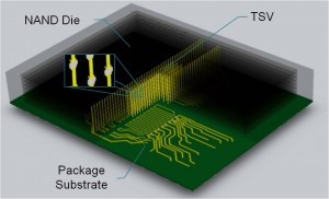
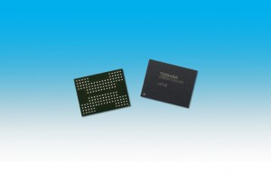
Toshiba x16 stacked nand flashToshiba has used through silicon vias (TSVs) to connect up to 16 stacked die in a range NAND flash chips.

The prototype will be shown at Flash Memory Summit in Santa Clara next week.

“Prior art stacked NAND flash memories are connected together with wire bonding in a package,” said the firm.

“TSV technology instead utilises the vertical electrodes and vias to pass through the silicon dies for the connection. This enables high-speed data input and output, and reduces power consumption.”

I/O data rate is >1Gbit/s with 1.8V to the core and 1.2V I/O.

High-end enterprise solid-state drives are a potential application.

New Energy and Industrial Technology Development Organization (NEDO) developed some of the technology.

toshstackPrototype specification:

package NAND dual x8 BGA-152 NAND dual x8 BGA-152
Gbyte 128 256
die stacked 8 16
width mm 14 14
depth 18 18
height 1.35 1.90
interface toggle DDR toggle DDR

steve bush

How to measure the productivity of your R&D dollar

26aug15Dundon, Gerald, ADIThere are two main difficulties about measuring the productivity of R&D: one is the length of time from initial spend to the moment the last sales dollar is delivered; the other is the difficulty of associating inputs to outputs – how do we know that what is discovered in the R&D process has led to the creation of a saleable product?

Thirty-year Analog Devices’ veteran Gerald Dundon has cracked this very tough nut in a book called R&D Productivity: How to target it. How to measure it. Why it matters.

At ADI, Dundon held the jobs of vice-president of supply chain and planning, vice-president of quality, and vice-president of new product productivity.

You would think the amount of revenue coming from new products is a valid metric for R&D efficiency but you would be wrong, says Dundon.

He regards discounted cash flow as an inadequate metric for R&D project evaluation.

He explains why R&D spend should be included in return-rate calculations, how cumulative revenue can be modelled and predicted and how product lifecycles influence target rate returns – too short a product lifecycle means you’re ‘living on the edge’, says Dundon.

This is a heavyweight book for semiconductor management and it answers one of the most difficult questions the industry has to face: how do you create a business out of R&D.


david manners

Diablo puts flash into servers

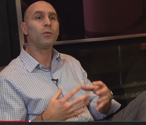
Diablo CEO Riccardo Badalone

Diablo CEO Riccardo Badalone

Diablo Technologies’ Memory1, an all-flash server system memory technology, puts 4TBytes of memory in slots that currently hold 128Gbytes or 384Gbytes, the company said.

By delivering greater capability on fewer servers it claims to reduce data centre costs by up to 70%.

Memory1 is shipping now to select customers and will be more widely available later in the year.

“Memory1 represents a major evolution in server architecture,” says Diablo CEO Riccardo Badalone. “The needs of the large-scale datacenter are changing, with a very sharp focus on increasing capability to win the internet while managing tight constraints on cost and power. The Memory1 platform allows customers to leverage NAND flash as pure system memory in a seamless manner, with no changes to their hardware and software stacks. The business impact on datacentre economics and application performance is dramatic. We’ve seen customers envisioning everything from aggressive server consolidation all the way to doubling and tripling individual machine profit.”

Memory1 brings the low cost and high capacity of flash to large-scale enterprise and datacenter customers, he said. It is suitable for environments that require large memory footprints per server for workloads, such as big data analytics and complex web applications.

The average Memory1 use case enables a four-to-one server reduction, and one customer use case requires 90% fewer servers.

Diablo will initially focus on delivering Memory1 to cloud and hyperscale datacenters, which stand to see significant economic benefits because of their scale.

david manners

Diablo puts flash into servers

Diablo CEO Riccardo Badalone

Diablo CEO Riccardo Badalone

Diablo Technologies’ Memory1, an all-flash server system memory technology, puts 4TBytes of memory in slots that currently hold 128Gbytes or 384Gbytes, the company said.

By delivering greater capability on fewer servers it claims to reduce datacentre costs by up to 70%.

Memory1 is shipping now to select customers and will be more widely available later in the year.

“Memory1 represents a major evolution in server architecture,” says Diablo CEO Riccardo Badalone. “The needs of the large-scale datacenter are changing, with a very sharp focus on increasing capability to win the internet while managing tight constraints on cost and power. The Memory1 platform allows customers to leverage NAND flash as pure system memory in a seamless manner, with no changes to their hardware and software stacks. The business impact on datacentre economics and application performance is dramatic. We’ve seen customers envisioning everything from aggressive server consolidation all the way to doubling and tripling individual machine profit.”

Memory1 brings the low cost and high capacity of flash to large-scale enterprise and datacenter customers, he said. It is suitable for environments that require large memory footprints per server for workloads, such as big data analytics and complex web applications.

The average Memory1 use case enables a four-to-one server reduction, and one customer use case requires 90% fewer servers.

Diablo will initially focus on delivering Memory1 to cloud and hyperscale datacenters, which stand to see significant economic benefits because of their scale.

david manners

Plessey selling GaN-on-Si LED die

Plessey 4.5mm high power die

Plessey 4.5mm high power die

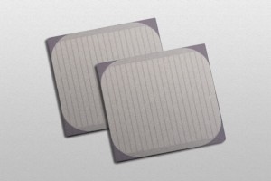
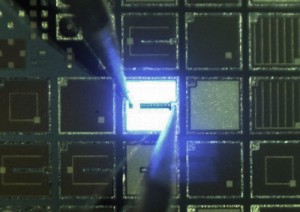
Today Plessey announced the release of its range of GaN-on-Si MaGIC LED die.

The blue die, sometimes referred to as blue pump for their ability to pump phosphor to a white colour range, are the latest innovation in high brightness LED die designed for a wide range of medium to high power applications including general lighting, signage, commercial, residential and street lighting.

“We have developed a wide range of LED die for a number of applications and our GaN-on-Silicon technology works particularly well in higher power applications such as high bay, street lights, projector lamps, spot lamps and floodlighting,” says Plessey CTO Keith Strickland. “This process technology will become the base for our application-specific LEDs, the ASLED, which bridges the gap between LED component suppliers, solid state lighting fixture designers and the OEMs.”

The manufacturing process produces a vertical LED structure which has the anode as bottom contact and the cathode formed in the top metal layer. The layout of the top metal layer is optimised for a particular LED size and die operating current, and includes one or more bond pads for connecting to the cathode.

Plessey offers its range of blue die in various wavelength options. Capable of generating over 60% light output efficiency, sometimes referred to as wall plug efficiency (WPE), the die are supplied to a standard thickness of 150μm, while other thicknesses can be supplied, down to a minimum of 75μm.

The die are supplied on a blue tape in single intensity and colour bins to provide close uniformity, and are intended to be used with standard pick and place machines.

Samples are available in a variety of die pack formats with blue die wavelengths ranging from 420nm to 480nm and from mW to 10W with the PExS4500 range having a typical optical output power of 4000mW from a 3A drive current.

david manners

Plessey selling GaN-on-Si LED die


Plessey's GaN-on-Silicon MaGIC LED die

Plessey’s GaN-on-Silicon MaGIC LED die

Today Plessey announced the release of its range of GaN-on-Silicon MaGIC LED die.

The blue die, sometimes referred to as blue pump for their ability to pump phosphor to a white colour range, are the latest innovation in high brightness LED die designed for a wide range of medium to high power applications including general lighting, signage, commercial, residential and street lighting.

“We have developed a wide range of LED die for a number of applications and our GaN-on-Silicon technology works particularly well in higher power applications such as high bay, street lights, projector lamps, spot lamps and floodlighting,” says Plessey CTO Keith Strickland. “This process technology will become the base for our application-specific LEDs, the ASLED, which bridges the gap between LED component suppliers, solid state lighting fixture designers and the OEMs.”

The manufacturing process produces a vertical LED structure which has the anode as bottom contact and the cathode formed in the top metal layer. The layout of the top metal layer is optimised for a particular LED size and die operating current, and includes one or more bond pads for connecting to the cathode.

Plessey offers its range of blue die in various wavelength options. Capable of generating over 60% light output efficiency, sometimes referred to as wall plug efficiency (WPE), the die are supplied to a standard thickness of 150μm, while other thicknesses can be supplied, down to a minimum of 75μm.

The die are supplied on a blue tape in single intensity and colour bins to provide close uniformity, and are intended to be used with standard pick and place machines.

Samples are available in a variety of die pack formats with blue die wavelengths ranging from 420nm to 480nm and from mW to 10W with the PExS4500 range having a typical optical output power of 4000mW from a 3A drive current.

david manners

Optical transistor will be faster than CMOS devices

This rendering depicts a new "plasmonic oxide material" that could make possible devices for optical communications that are at least 10 times faster than conventional technologies. (Purdue University image/Nathaniel Kinsey)

This rendering depicts a new “plasmonic oxide material” that could make possible devices for optical communications that are at least 10 times faster than conventional technologies. (Purdue University image/Nathaniel Kinsey)

Researchers in the US have demonstrated what is in effect an ‘optical transistor’ which can modulate light, as in optical fibre communications, at terahertz frequencies.

The team at Purdue University claim that the so-called “plasmonic oxide material” could make possible devices for optical communications that are at least 10 times faster than conventional technologies.

The optical material made of aluminum-doped zinc oxide (AZO) which can modulate a light signal by 40%, has been shown to work in the near-infrared range of the spectrum, which is used in optical communications.

Significantly, the fabrication process is compatible with a CMOS manufacturing process, which opens the way to commercial devices.

The researchers have proposed creating an “all optical plasmonic modulator using CMOS-compatible materials,” or an optical transistor.

The switching speed of transistors is limited by how fast it takes conventional semiconductors such as silicon to complete this cycle of light to be absorbed, excite electrons, produce holes and then recombine.

“So what we would like to do is drastically speed this up,” said doctoral student Nathaniel Kinsey.

This cycle takes about 350 femtoseconds to complete in the new AZO films, which is roughly 5,000 times faster than crystalline silicon and so fleeting that light travels only about 100 microns, or roughly the thickness of a sheet of paper, in that time.

“We were surprised that it was this fast,” said Kinsey.

The increase in speed could translate into devices at least 10 times faster than conventional silicon-based electronics.

The AZO films are said to be “Epsilon-near-zero,” meaning the refractive index is near zero, a quality found normally in metals and new “metamaterials,” which contain features, patterns or elements that enable unprecedented control of light by harnessing clouds of electrons called surface plasmons.

The pulsing laser light changes the AZO’s index of refraction, which, in turn, modulates the amount of reflection and could make higher performance possible.

“If you are operating in the range where your refractive index is low then you can have an enhanced effect, so enhanced reflection change and enhanced transmission change,” he said.

The ongoing research is based at Purdue’s Birck Nanotechnology Center and is funded by the Air Force Office of Scientific Research, a Marie Curie Outgoing International Fellowship, the National Science Foundation, and the Office of Naval Research.

Findings were detailed in a research paper appearing in July in the journal Optica, published by the Optical Society of America.

Richard Wilson

Stanene: two-dimensional tin

Two-dimensional tin, Stanene, has been fabricated by a Chinese-American team. It is potentially a large band-gap semiconductor with unusual properties that include topological superconductivity and near-room-temperature quantum anomalous Hall effect, according to the Nature Materials paper ‘Epitaxial growth of two-dimensional stanene‘.

Topological superconductivity is the free conduction of electrons along the outside edges of a two dimensional material.

Stanene now joins 2D silicon (silicene) and 2D germanium (germanene) from group IV of the periodic table.

The team found a suitable hexagonal crystal to grow it on – (111) Be2Te3 – and deposited it using molecular beam epitaxy – MBE was how other teams managed to fabricates silicene and germanene, and germanene has also been made by mechanical exfoliation.

What grows is not totally flat like graphene, but a molecule with a regular slight buckle – every second atom is either slightly up or slightly down from the molecular plane – resembling two layers when viewed from the side. The height difference is around 0.1nm.

This is early days for the material, which interacted with the substrate and could not be measured in isolation. Work with the bare substrate, the substrate plus stanene, and then further over-coated with potassium, allowed theoretical models to be confirmed and improved. “The synthesis of stanene and its derivatives will stimulate further experimental investigation of their theoretically predicted properties”, said researchers in the paper’s abstract.

Scientists took part from: Shanghai Jiao Tong University, Stanford University, Tsinghua University, Collaborative Innovation Center of Quantum Matter (Beijing) and Collaborative Innovation Center of Advanced Microstructures (Nanjing).


steve bush