Plessey retrofitting with its own lighting LEDs

Plessey is retrofitting its Plymouth manufacturing facility with LEDs and lighting modules made on-site.

Plessey is retrofitting its Plymouth manufacturing facility with LEDs and lighting modules made on-site.

Plessey is retrofitting its Plymouth manufacturing facility with LEDs and lighting modules made on-site.

It will replace fluorescent tubes and compact fluorescent bulbs in existing fixtures – approximately 2,700 fixtures replacing 4,200 fluorescent lamps – for which it has designed retrofit kits.

“LED retrofit kits offer the facilities engineers and installation contractors a cost effective, quick and easy method to take advantage of the new technology, said Plessey facilities engineer Thomas Abbott. “It only takes five to 10 minutes to retrofit a fixture.”

There are three main types of fixture: batten, pod-style down-light and reflector ceiling troffer, plus high bay and low bay HID fixtures.

Current site lighting power consumption per year is 1,000,000kW/h costing £100,000, said the firm, plus approximately £5,000 in materials and 200 man hours annually.

“Once the retrofit is completed, the company would expect to see 25% – 40% reduction in lighting electricity consumption, saving tens of thousands of pounds per year,” said Plessey.

See alsoPlessey selling GaN-on-Si LED die

See alsoPlessey goes into LED light bulb ‘filament’ production

View more Plessey stories on Electronics Weekly »


steve bush

LED street lights need better lightning protection, says Osram

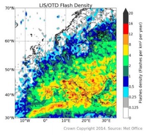
Lightning density in Europe differs significantly from region to region.

Lightning density in Europe differs significantly from region to region.

The introduction of LED street lighting has raised a new problem. How can the electronic drivers be protected from voltage peaks from lightning strikes.

The problem with LED lighting modules is that they operate at lower voltage levels and could be damaged from overvoltage.

According to LED supplier Osram, this danger has increased with the UN Climate Council identifying increasing levels of lightning worldwide in its fifth assessment report (IPCC14).

“Around 10% of the several million lightning strikes occurring each day impact on the ground, thereby causing voltage peaks. To effectively protect LED modules assembled in road luminaires, the Osram Optotronic 4DIM features overvoltage protection of 8 kilovolts as standard,” said Osram.

Levels of lightning density in Europe are high in summer, particularly in July and August, and with large regional differences – the UK Meteorological Office recorded between just 0.25 and over 20 strikes per square kilometre in 2014.

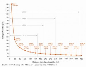
Osram believes that it is necessary for the electronic control units to have voltage protection of up to 8kV between mains supply and ground in protection classes I and II.

“This means that lightning can strike an area of up to 200 metres from a luminaire mast without the LED module being damaged,” said the supplier.

Osram has designed 8kV protection into its LED controllers with a so-called EQUI connection (equipotential) for protection class II applications, which it claims can reduce the occurrence of overvoltage on the LED module.

Overvoltage though does not automatically mean the immediate failure of an LED module, but can cause premature ageing and therefore shorter operating periods; this has consequences for the operator in terms of costs.

Graph shows 8kV overvoltage protection provided by the Optotronic 4 DIM from Osram.

Graph shows 8kV overvoltage protection provided by the Optotronic 4 DIM from Osram.

Normally, LED solutions have low failure rates and achieve up to 100,000 operating hours.

The LED control units also need to be protected from voltage peaks from two other hazardous sources: – those with up to 6kV due to load changes or switching commands in the power supply grid and from electrostatic discharge (ESD) occurring with for example maintenance work, if no ESD protective measures exist.


Richard Wilson

Display makers see shakeout in ITO replacement market

plainheadshot139

Dr Khasha Ghaffarzadeh

The market transparent conductive film which is used in the production of displays, solar cells and touch screens, will reach $1.2bn in 2025 at the film level (ITO-on-glass, LCD and OLED displays are excluded), writes Dr Khasha Ghaffarzadeh, head of consulting, IDTechEx.

Displays and solar cells need light to enter at least one side of the device. At the same time, they have to close a circuit and therefore require a transparent conductive film (TCF).

The mainstay material is indium tin oxide (ITO) on glass, which has proven excellent but has several short comings. For example, for larger area touch screens, ITO becomes too resistive for desired rapid response touch sensing.

For the new wave of flexible displays, ITO also cracks under little strain. Additionally, indium supply is also heavily controlled. Therefore over 50 companies around the world, from small to large, have been pursuing replacing ITO, and over 10 types of solutions exist.

ITO on PET rather than glass will dominate, but ITO alternatives will reach a combined market value of $430m in 2025. This market will be very unevenly spread between different ITO alternative technologies with silver nanowires and metal mesh taking a lion’s share ($317m in 2025).

Touch-related applications currently dominate the sales of TCF films, although the end markets are beginning to change. Currently, the share of non-touch markets is <<5%, but IDTechEx Research expects it to reach a substantial 17% in 2025.

These emerging applications include smart windows, OLED lighting, emerging photovoltaics, reflective displays, and more. They, together with larger-sized or flexible touch screens, will shape the requirements landscape of this sector.

Challenging market conditions

Strong trends have long undermined the dominance of the incumbent, the ITO films. Most notable are trends towards lower sheet resistance, increased flexibility and reduced cost.

These trends continuously push ITO films towards or even beyond its performance limit, thus triggering the proliferation of ITO alternative (substitute) technologies and suppliers.

The incumbents have however responded using a two-pronged strategy: (1) doubling the production capacity worldwide and (2) slashing prices at the expense of profit margins.

The former strategy ensures that there no longer exists a tight supply-demand relationship, making this once again a strong buyers’ market. The latter strategy ensures that incumbents don’t lose a client solely on price. Indeed, they lower their prices piecemeal every time an alternative is to close a deal.

These are classic symptoms of a market characterized by a strong threat of substitutes. Here, the end customer is happy but the ITO alternative suppliers face make-or-break years, whilst ITO suppliers (incumbents) are now engaged in a low-margin game of share protection.

The market conditions were made more challenging because growth in emerging sectors in which ITO alternatives commanded a clear performance advantage undershot expectations.

We anticipate that these market forces will trigger a consolidation phase in the industry during which ITO alternative leaders will emerge, whilst many poorly-funded and poorly-differentiated suppliers will disappear.

At the same time, we believe that the value proposition for leading ITO alternative technologies remains compelling. They will become a market reality although their journey will be slow because ITO films remain good enough for most existing applications. Therefore, at least initially, their success is linked to the growth of new types of devices, such as larger area devices.

The performance bar has been raised

Silver nanowires and metal mesh offer a lower sheet resistance than both ITO and other alternatives without significantly compromising optical quality. Their pricing strategy continues to be based on undercutting ITO to maintain a more-for-less value proposition, although this is becoming increasingly challenging.

In fact, they have increased the performance bar so high that the likes of carbon nanotubes and graphene will be blocked out of the main markets and be pushed towards niche use cases.

This suggests that developers of these technologies need to be imaginative again and build on their stronger differentiators such as stretchability, thermoformability, etc. This change of focus is already underway but will come too late for some.

The battle between metal mesh suppliers will be fought on narrowing the linewidth and improving throughput and yield (biggest cost unknown/driver). Amongst silver nanowire suppliers, haze was a point of contention, but now attention is focused on innovation at the formulation level. Here, the first mover advantage will also matter whilst the IP landscape is now no longer white, which further prevents access to new comers.

The next phase of innovation will focus on more hybrid systems and disruptive ways of patterning.

IDTechEx Research has released a new research study titled “Transparent Conductive Films (TCF) 2015-2025: Forecasts, Markets, Technologies”.


Richard Wilson

Electricity meter sticks on circuit breakers

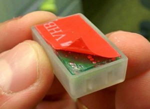
Berkely Labs stick-on electricity meterBerkeley Lab researchers have developed a peel-and-stick electricity meter which allows individual circuits in the home and industry to be accurately monitored.

It is an alternative to current transformers and live voltage connections that can be installed without mains voltage working expertise as the sensors are simply stuck to the front of each circuit breaker in a consumer unit. The only critical steps are aligning the sensor before sticking, and identifying the breaker type to the system so that calibration parameters can be loaded.

Each sensor is 19 x 12mm including a capacitive voltage pick-up and a Hall-effect current probe. They are daisy-chained with ribbon cable which supplies power (5V 16mA) and takes serial data back to a local wireless node – based on a Raspberry Pi in the experiment. This links with a remote laptop running system monitoring algorithms, written in Python.

Most circuit breakers have similar internal structures, which makes the technique broadly applicable. There are two types in the US, according to the Lab: bimetallic thermal and solenoid magnetic. The thermal type was chosen for testing because its lower magnetic field (10-20x) made it the toughest challenge for current sensing.

Inside, the voltage probe is the bottom layer of the internal PCB and the Hall sensor is an Allegro A1301. Both signals are conditioned by op-amp-based filters and fed into the 10bit ADC of a MSP430G2131 microcontroller for serialisation and transmission along the ribbon cable.

1,920sample/s are sent – a multiple of the 60Hz line frequency to simplify subsequent fast Fourier transforms, and fast enough for mains harmonics to be captured.

Time averaging is included to increase the signal-to-noise ratio of the Hall effect probe, and the laptop runs fairly complex power estimation algorithms that include software phase locked loops to track input waveforms. Calibration is required once per breaker type.

There is considerable cross-talk from adjacent circuit breakers, and an adaptive algorithm reduces errors from this to 5% after 15min of operation without any need for calibration via known loads.

Voltage measurements are within 1% of conventional contact probing, power below 10W can be resolved, and complex loads like triac dimmers can be handled.

More information on the algorithms is available in ‘COTS-Based Stick-On Electricity Meters for Building Submetering‘, published in the IEEE Sensors Journal.

steve bush

Merged memory company adds to fast flash line

Cypress HyperFlash_MemoryCypress Semiconductor has seen early benefits of its $5bn merger with Spansion with a new 256Mbit memory device added to the Spansion NOR HyperFlash product line.

HyperFlash is a high speed memory architecture which can achieve double-data-rate (DDR) read bandwidths as high as 333Mbyte/s for 1.8V products.

It is intended to provide a migration path from Quad SPI to dual Quad SPI to HyperFlash memory, offers 3.0V and 1.8V versions and includes three densities: 128, 256 and 512Mbit.

Hiro Ino, senior director of the NOR Flash product family at Cypress, sees a  trend toward instant-on systems for automotive, industrial and communication applications, and chipset manufacturers looking for a high-bandwidth, low-pin-count flash memory interface.

The HyperBus interface was introduced by Spansion last year for high speed, low pin-count NOR flash memory.

Processors that have been publically announced to support the HyperBus interface include the Freescale MAC57D5xx Automotive DIS MCU, the Cypress FM4 S6E2DH general purpose MCU and the Cypress Traveo S6J324C and S6J326C automotive MCUs.

The efficient 12-pin HyperBus interface consists of an 8-pin address/data bus, a differential clock (2 signals), a chip select and a read data strobe for the controller—all of which help reduce the overall cost of the system through reduced pin count.

The new S26KL256S HyperFlash device is available in a 48-mm2 24-ball package, and has an extended temperature range of -40ºC to +125ºC.


Richard Wilson

LTC double-balanced mixer can be up or down-converter

LTC5549 typical application

LTC5549 typical application

Linear Technology announces the LTC5549, a double-balanced mixer that can operate either as an up-converter or down-converter, with a very wide RF frequency range from 2GHz to 14GHz.

The mixer has a linearity of 24.4dBm IIP3 at 9GHz.

It is aimed at microwave transmitter and receiver designs with its integrated LO buffer that needs only a 0dBm drive level, effectively eliminating an external high power LO amplifier circuit.

The device also has an integrated on-chip, switchable frequency doubler for LO signal, providing an option to use lower cost, commonly available low frequency synthesizers.

The LTC5549 employs wideband integrated balun transformer optimized to extend RF frequency bandwidth from 2GHz to 14GHz while enabling single-ended operation. Its IF port also has wide bandwidth up to 6GHz.

All three ports are 50Ω matched. The mixer offers high port-to-port isolation, minimizing undesireable LO leakage, and easing external filtering requirements.

​The LTC5549’s performance enhances a wide range of microwave applications including microwave backhaul, high unlicensed band LTE-Advanced base stations, satellite broadband radios, radar systems, X-band and Ku band transceivers, test equipment and satellite modems.

The LTC5549 offers improved ESD protection with its 2,000V ESD human body model (HBM) rating on all pins. The device is available in a tiny 12-lead, 3mm x 2mm plastic QFN package. With its minimal external component design, the LTC5549 results in a compact solution footprint. The device is rated for operation from –40°C to 105°C case temperature to support extended environmental operating temperature.

The mixer is optimized for single 3.3V supply operation, drawing a nominal supply current of 115mA.

Additionally, the LTC5549 has an enable pin to disable the IC. When deactivated, the device draws only 100μA maximum standby current. The enable pin can be driven directly to turn the device on and off rapidly in less than 0.2μs, supporting time-division duplex (TDD) or burst mode type radios.

The LTC5549 is priced starting at $10.07 each in 1,000-piece quantities. Samples and production quantities are available immediately.

david manners

Molecular diode with 200:1 conduction ratio

Berkeley diode Jeff Neaton

Columbia University and Berkeley Labs have created a molecular diode with a forward/reverse current ratio in excess of 200 at fixed voltage

Columbia University and Berkeley Labs have created a molecular diode with a forward/reverse current ratio in excess of 200 at fixed voltage.

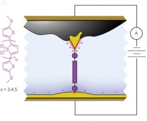
The molecule, designed at Columbia, is an oxidised thiophene derivative, with molecular resonance in nearly perfect alignment with the Fermi electron energy levels of the gold electrodes, according to Berkeley Labs.

It is a symmetrical molecule in an ionic solution, with asymmetry coming from different sized gold electrodes – see diagram.

“Electron flow at molecular length-scales is dominated by quantum tunnelling,” said Jeff Neaton, director of Berkeley Labs’ Molecular Foundry. “The ionic solution, combined with the asymmetry in electrode areas, allows us to control the junction’s electrostatic environment simply by changing the bias polarity. In addition to breaking symmetry, double layers formed by ionic solution also generate dipole differences at the two electrodes, which is the underlying reason behind the asymmetric shift of molecular resonance.”

Work at Columbia confirmed no rectification happened in non-ionic solution.

“We expect the understanding gained from this work to be applicable to ionic liquid gating in other contexts, and mechanisms to be generalised to devices fabricated from two-dimensional materials,” said Brian Capozzi of Columbia, adding that the molecular circuit is also revealing new routes to charge and energy flow at the nanoscale.

The work is convered by a Nature Nanotechnology paper: ‘Single-molecule diodes with high rectification ratios through environmental control’.

Image: Jeff Neaton, director of Berkeley Labs

steve bush

Molecular diode with 200:1 conduction ratio

Berkeley diode Jeff NeatonColumbia University and Berkeley Labs have created a molecular diode with a forward/reverse current ratio in excess of 200 at fixed voltage.

The molecule, designed at Columbia, is an oxidised thiophene derivative, with molecular resonance in nearly perfect alignment with the Fermi electron energy levels of the gold electrodes, according to Berkeley Labs.

It is a symmetrical molecule in an ionic solution, with asymmetry coming from different sized gold electrodes – see diagram.

“Electron flow at molecular length-scales is dominated by quantum tunnelling,” said Jeff Neaton, director of Berkeley Labs’ Molecular Foundry. “The ionic solution, combined with the asymmetry in electrode areas, allows us to control the junction’s electrostatic environment simply by changing the bias polarity. In addition to breaking symmetry, double layers formed by ionic solution also generate dipole differences at the two electrodes, which is the underlying reason behind the asymmetric shift of molecular resonance.”

Work at Columbia confirmed no rectification happened in non-ionic solution.

“We expect the understanding gained from this work to be applicable to ionic liquid gating in other contexts, and mechanisms to be generalised to devices fabricated from two-dimensional materials,” said Brian Capozzi of Columbia, adding that the molecular circuit is also revealing new routes to charge and energy flow at the nanoscale.

The work is convered by a Nature Nanotechnology paper: ‘Single-molecule diodes with high rectification ratios through environmental control’.

steve bush

Infineon overtakes ST

Top 20 Semiconductor sales

Top 20 Semiconductor sales

Infineon has overtaken ST to become Europe’s largest chip company – Infineon’s Q2 sales were $1.762 billion while ST’s were $1.754 billion, according to IC Insights.

Samsung continues to close the gap on Intel with revenues of $10.3 billion in the quarter compared with Intel’s $11.96.

Top Ten Vendors Q2 2015

$bn

Intel 11.946
Samsung 10.3
TSMC 6.6
Hynix 4.2
Qualcomm 3.9
Micron 3.8
TI 3.0
Toshiba 2.8
Broadcom 2.1
Infineon 1.762

The company writes:

IC Insights includes foundries in the top 20 semiconductor supplier ranking since it has always viewed the ranking as a top supplier list, not a marketshare ranking, and realizes that in some cases the semiconductor sales are double counted.  With many of our clients being vendors to the semiconductor industry (supplying equipment, chemicals, gases, etc.), excluding large IC manufacturers like the foundries would leave significant “holes” in the list of top semiconductor suppliers.  As shown in the listing, the foundries and fabless companies are clearly identified.  In the April Update to The McClean Report, marketshare rankings of IC suppliers by product type were presented and foundries were excluded from these listings.

See more IC Insights stories on Electronics Weekly »


david manners