Open source virtual reality headset uses ARM-based SoC

OSVR

OSVR

A development kit for designing a virtual reality headset for game-players from 0pen-source software has been introduced by the Open-Source Virtual Reality Consortium.

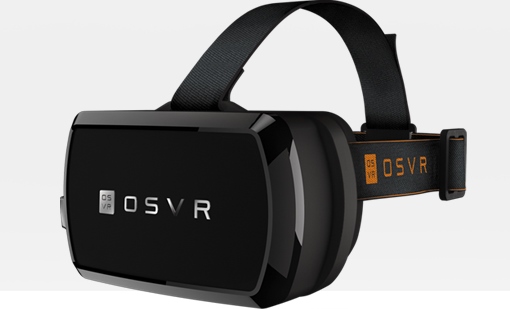
Called the Open-Source Virtual Reality (OSVR) Hacker Development Kit, it provides a modular platform designed around an FPGA-based All Programmable SoC from Xilinx.

The ARM-processors based SoC carries out the video processing and controls data collected by the headset’s many sensors.

“This allows developers to make tweaks for added functionality like multiple sensors and algorithms for computer vision processing,” said Lau Lee Yang, senior director for OSVR business development at Razer, the company behind the kit.

The kit includes a positioning and head tracking device, a display, and double lens optics.

“In the near future the Hacker Development Kit will also be able to offload software processing tasks such as optical distortion correction using its hardware and potentially perform image enhancement functions,” said Lee Yang.

The OSVR Hacker Development Kit has started shipping to selected developers.


Richard Wilson

Digital power chip gets PWM signalling feature

linearLinear Technology has added a three-state PWM signalling feature to its LTC3887 range of dual output synchronous step-down DC/DC controllers with I²C-based PMBus interface.

The intention of adding the PWM signal is to support the use of DrMOS, power blocks or similar power stages.

The LTC3887-1 also has a faster 70ms power-up time and a fast ADC mode that provides an 8ms update rate for one parameter.

The controller can be used to regulate two independent outputs or can be configured for a 2-phase single output from 0.5V to 5.5V.

Up to six phases can be interleaved and paralleled for sharing among multiple ICs. The result is a reduced need for input and output filtering in high current or multiple output applications, says Linear.

The voltage controller operates over an input voltage ranging from 4.5V to 24V, and it produces ±0.50% accurate output voltages from 0.5V to 5.5V with output currents up to 40A per phase over the full operating temperature range.

The device is available in a 40-pin 6mm x 6mm QFN package with an operating junction temperature range from -40°C to 125°C.

Richard Wilson

Digital power chip gets PWM signalling feature

linearLinear Technology has added a three-state PWM signalling feature to its LTC3887 range of dual output synchronous step-down DC/DC controllers with I²C-based PMBus interface.

The intention of adding the PWM signal is to support the use of DrMOS, power blocks or similar power stages.

The LTC3887-1 also has a faster 70ms power-up time and a fast ADC mode that provides an 8ms update rate for one parameter.

The controller can be used to regulate two independent outputs or can be configured for a 2-phase single output from 0.5V to 5.5V.

Up to six phases can be interleaved and paralleled for sharing among multiple ICs. The result is a reduced need for input and output filtering in high current or multiple output applications, says Linear.

The voltage controller operates over an input voltage ranging from 4.5V to 24V, and it produces ±0.50% accurate output voltages from 0.5V to 5.5V with output currents up to 40A per phase over the full operating temperature range.


The device is available in a 40-pin 6mm x 6mm QFN package with an operating junction temperature range from -40°C to 125°C.


Richard Wilson

MIT refreshes fusion reactors with modern superconductors

MIT ARC nuclear fusion reactorRare-earth barium copper oxide (REBCO) superconducting tapes could mean earlier practical fusion reactors, according to MIT.

The key is stronger magnetic fields, which shrink the size of tokamak [chamber] required, and subsequently simplify all that follows.

It “just ripples through the whole design. It changes the whole thing,” said MIT nuclear scientist Professor Dennis Whyte.

Fusion power increases with the fourth power of magnetic field, so 2x field produces 16x power. “Any increase in the magnetic field gives you a huge win,” said post-grad Brandon Sorbom.

2x magnetic field is not available with REBCO, but there is enough for 10x fusion power, said MIT.

By combining REBCO magnets with known fusion principles, the team has designed a research reactor, and potential prototype power plant, and described it in a paper in the journal Fusion Engineering and Design.

It is half the diameter of the ITER fusion reactor to be built in France (designed before the REBCO superconductors), power output would be the same without any any new physics. “We’re not extrapolating to some brand-new regime,” said Whyte.

As with ITER, continuous operation would be possible.

Suiting it to research, the core of the MIT reactor can be removed without dismantling the entire machine.

Liquid rather than solid materials surround the fusion chamber allowing easy circulation and replacement. “It’s an extremely harsh environment for [solid] materials,” said Whyte.

Tokamak Energy

Tokamak Energy

“Devices of a similar complexity and size have been built within about five years,” said MIT.

Estimates are that power out would be 3x power in, increasing to five or six times with improvements in the design.

UK firm Tokamak Energy is proposing something very similar.

steve bush

MIT refreshes fusion reactor with modern superconductors

MIT ARC nuclear fusion reactorRare-earth barium copper oxide (REBCO) superconducting tapes could mean earlier practical fusion reactors, according to MIT.

The key is stronger magnetic fields, which shrink the size of tokamak [chamber] required, and subsequently simplify all that follows.

It “just ripples through the whole design. It changes the whole thing,” said MIT nuclear scientist Professor Dennis Whyte.

Fusion power increases with the fourth power of magnetic field, so 2x field produces 16x power. “Any increase in the magnetic field gives you a huge win,” said post-grad Brandon Sorbom.

2x magnetic field is not available with REBCO, but there is enough for 10x fusion power, said MIT.

By combining REBCO magnets with known fusion principles, the team has designed a research reactor, and potential prototype power plant, and described it in a paper in the journal Fusion Engineering and Design.

It is half the diameter of the ITER fusion reactor to be built in France (designed before the REBCO superconductors), power output would be the same without any any new physics. “We’re not extrapolating to some brand-new regime,” said Whyte.

As with ITER, continuous operation would be possible.

Suiting it to research, the core of the MIT reactor can be removed without dismantling the entire machine.

Liquid rather than solid materials surround the fusion chamber allowing easy circulation and replacement. “It’s an extremely harsh environment for [solid] materials,” said Whyte.

Tokamak Energy

Tokamak Energy

“Devices of a similar complexity and size have been built within about five years,” said MIT.

Estimates are that power out would be 3x power in, increasing to five or six times with improvements in the design.

UK firm Tokamak Energy is proposing something very similar.

steve bush

Keysight joins 5GIC project in UK via Anite

Anite Nemo Outdoor - Keysight joins 5GIC project in UK via Anite

Keysight joins 5GIC project in UK via Anite

Keysight Technologies’ latest acquisition, Anite is also now the latest test firm to become a partner in the 5G Innovation Centre (5GIC) at the University of Surrey. This is the UK’s largest collaborative research programme into the technology for 5G mobile communications.

Keysight paid $600m in cash for Anite, which supplies development software for wireless. It will contribute channel emulation and protocol testing software tools for the 5GIC project.

Professor Rahim Tafazolli, Head of the 5G Innovation Centre commented:

“Anite’s contribution to our 5G research programme will enable the development and testing of future technologies in a real environment and in an end to end manner.”

This is not the only 5G research project using Anite’s radio channel emulators.

Earlier this year, Anite announced that the Anite-led task group within the METIS project finalised the world’s first 5G radio channel models.

The 5GIC, which houses 170 researchers in a purpose-built building on Surrey University campus, is funded by £12m from the Higher Education Funding Council for England and over £68m co-investment from the Centre’s industry and regional partners.

Partners include Aircom, BBC, BT, Cobham, EE, Fujitsu, Huawei, Imagination, Rohde & Schwarz, Samsung, Telefonica and Vodafone.

See alsoBlu Wireless WiGig comes to 5G Innovation Centre


Richard Wilson

Keysight joins 5GIC project in UK via Anite

Anite Nemo Outdoor - Keysight joins 5GIC project in UK via Anite

Keysight joins 5GIC project in UK via Anite

Keysight Technologies’ latest acquisition, Anite is also now the latest test firm to become a partner in the 5G Innovation Centre (5GIC) at the University of Surrey. This is the UK’s largest collaborative research programme into the technology for 5G mobile communications.

Keysight paid $600m in cash for Anite, which supplies development software for wireless. It will contribute channel emulation and protocol testing software tools for the 5GIC project.

Professor Rahim Tafazolli, Head of the 5G Innovation Centre commented:

“Anite’s contribution to our 5G research programme will enable the development and testing of future technologies in a real environment and in an end to end manner.”

This is not the only 5G research project using Anite’s radio channel emulators.

Earlier this year, Anite announced that the Anite-led task group within the METIS project finalised the world’s first 5G radio channel models.

The 5GIC, which houses 170 researchers in a purpose-built building on Surrey University campus, is funded by £12m from the Higher Education Funding Council for England and over £68m co-investment from the Centre’s industry and regional partners.

Partners include Aircom, BBC, BT, Cobham, EE, Fujitsu, Huawei, Imagination, Rohde & Schwarz, Samsung, Telefonica and Vodafone.

See alsoBlu Wireless WiGig comes to 5G Innovation Centre


Richard Wilson

Toshiba shipping wireless charger IC

imageToshiba is shipping a wireless power receiver IC that will enable mobile devices to be charged wirelessly as fast as if they were connected to the charger via a cable.

The TC7764WBG is compliant with Qi V.1.1.2, the wireless low power charging standard defined by the Wireless Power Consortium (WPC), which includes a dedicated specification for smartphones and mobile accessories.

Wireless charging allows adoption of a fully insulated case free of exposed charging ports, an advantage that is stimulating demand for waterproof and dustproof smartphones and other mobile devices. However, wireless charging has not always been as fast as charging by cable.

Toshiba has addressed this problem by optimizing the circuit design of the TC7764WBG compared to its predecessor products, enabling maximum output power of 5W and maximum power conversion efficiency of 95 percent1. This will allow wireless charger makers utilizing the new IC to achieve performance as fast as that offered by cabled chargers, with added benefits.

To ensure mobile device safety, the new IC integrates a protocol authentication circuit for power transfers, foreign object detection functions, under-voltage lockout (UVLO) and over voltage detection (OVLO) functions, as well as thermal shutdown function (TSD). The IC is housed in a WCSP28 package measuring 2.4mm by 3.67mm by 0.5mm.

david manners