Precision and no drift from ADI’s 55V op-amp

Analog Devices ADA4522 - a 55V, low-noise, zero-drift, precision op-amp

Analog Devices ADA4522 – a 55V, low-noise, zero-drift, precision op-amp

Analog Devices has introduced a 55V, low-noise, zero-drift, precision op-amp that includes electro-magnetic interference (EMI) filtering and needs no calibration circuitry.

Called ADA4522-2, the dual channel device is the first of a series.

Operation is over ±2.25V to ±27.5V, or 4.5 to 55V single supply, with the most negative rail included in the input range. Supply current per amplifier is a creditable 830uA. Output is rail-to-rail.

The important figures are:

  • noise: 5.8nV/√Hz (typ) @ 1kHz
  • 5uV max offset @ 25ºC
  • 22nV/ºC max offset voltage drift
  • 2.7MHz gain-bandwidth product.

Chopper stabilisation accounts for some of those parameters, with chopping at 1.5MHz for wide closed-loop bandwidth and easy filtering.

Instrumentation applications include front ends for: LCR meter, megohmmeter, load cell, bridge transducers, magnetic force balance scales, current shunts, thermocouples, RTD sensors and PLC input and output amplifiers

Electronic loads, power supplies, motor control and offset correction in composite amplifiers are possible end applications.

ADI has produced an informative white paper on its chopper-stabilising technique.

Packaging is 8pin SOIC or MSOP, and a 14 pin version, probably a quad, is due out in September in TSSOP or SOIC-14.

steve bush

IDF: Microchip adds authentication security to IoT devices

Microchip will implement IC authentication security developed by Intel into its chips for IoT applications

Microchip will implement IC authentication security developed by Intel into its chips for IoT applications

Microchip Technology says it will implement IC authentication security developed by Intel into its chips for IoT applications.

The whole area of IoT where devices such as smart meters and health sensors are connected to the internet to transfer data has raised the issue of data security.

Many chip firms are implementing security techniques such as authentication and processor partitioning into their devices.

Intel’s device authentication technology called Enhanced Privacy ID is intended to allow a service provider when setting up a connection to an IoT device to verify that an end user is authorised to access the service.

For the user of the IoT device the EPID protocol should mean they do not need to reveal their identity to an internet service provider.

According to Lorie Wigle, general manager of Internet of Things Security at Intel, the technology will mean users of Microchip’s devices will be able to “maintain end-to-end security and privacy in their IoT products and services, which helps them to protect data from device to cloud, minimizes unauthorized access of endpoints and gateways, and will promote a common security framework for IoT platforms.”

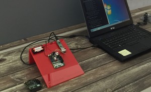
At the Intel Developer Forum this week in San Francisco, the Intel EPID protocol was demonstrated running on Microchip’s IoT Security Platform (pictured)

“Microchip has long recognised the importance of security in IoT applications,” said Ian Harris, vice president of Microchip’s Computing Products Group.

It is a group signature scheme that allows a platform to sign objects without uniquely identifying the platform or linking different signatures. Instead, each signer belongs to a ‘group’, and verifiers use the group’s public key to verify signatures.

EPID supports two modes of signatures:

  • Fully anonymous: an EPID verifier cannot associate a given signature with a particular member of the group.
  • Pseudonymous: an EPID verifier has the ability to determine whether it has verified the platform previously.


Richard Wilson

IDF: Intel gives transistor-less cross point memory a name

The transistor-less 3D XPoint non-volatile memory technology - Micron-3d-NAND

The transistor-less 3D XPoint non-volatile memory technology – Micron-3d-NAND

Intel has given an indication at Intel Developer Forum (IDF) in San Francisco this week when the transistor-less 3D XPoint non-volatile memory technology it has been developing with Micron, will appear in commercial products.

A range of solid state drives (SSDs) which implement the 3D memory technology will be introduced in 2016.

Intel has also given the non-volatile memory a new brand name, Optane.

Intel and Micron have made big claims for the non-volatile memory which they say will be up to 1,000 times faster and has up to 1,000 times greater endurance than NAND flash.

The companies also say it has the potential to have 10 times the density of conventional memory.

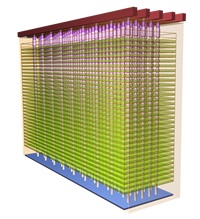
The “3D” memory is based on a new transistor-less cross point architecture which creates a three-dimensional checkerboard where memory cells sit at the intersection of word lines and bit lines, allowing the cells to be addressed individually.

The consequence of this, says Intel, is that data can be written and read in small sizes, leading to faster and more efficient read/write processes.

It seems the market will start putting the technology to the test when it sees first sample 128Gbit memory devices later this year and commercial production should follow in 2016 under the Optane brand.


Richard Wilson

Microchip expands small footprint PIC32 family

Microchip adds large flash MCUs to its 32bit MIPS M4K-based PIC32 MX1/2 MCU family.

Microchip adds large flash MCUs to its 32bit MIPS M4K-based PIC32 MX1/2 MCU family.

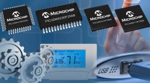
Microchip has added a set of small footprint large flash MCUs to its 32bit MIPS M4K-based PIC32 MX1/2 MCU family.

Called the PIC32MX230F256 series, it comes in 28 and 44 pin packages, clocks at 50MHz (83 DMIPS) and has 256kbyte flash and 16kbyte ram.

There is also Microchip’s 8bit Parallel Master Port (PMP) for graphics or external memory, a 10bit, 1Msample/s 13 channel ADC, SPI serial, I2S serial and USB (device, host or OTG (on-the-go)).

“Designers seeking to launch consumer products with capacitive touch screens, touch buttons or sliders, as well as USB device/host/OTG connectivity, can benefit from the functionality of the PIC32MX1/2 series of MCUs,” said the firm.

Suffixes B and D denote 28 and 44 pin devices respectively, and PIC32MX130F256 has been introduced for those not requiring USB OTG.

Package options are: 28pin QFN, SPDIP and SSOP, or 44pin QFN, TQFP and VTLA.

To use the firm’s Explorer 16 Development Board with the chip, the ‘PIC32MX270F256D Plug-in-Module’ (MA320014) is required.

As usual, Microchip’s MPLAB X integrated development environment (IDE) covers the devices, as does MPLAB XC32 Compiler for PIC32, and there is other development hardware. The firm’s Harmony collection of third-party middleware, drivers, libraries and real-time operating systems (RTOS) also applies, including USB stacks, graphics libraries and touch libraries.

steve bush

Yocto Linux SBC adds modules for prototyping

Habey has designed the Linux board around a Freescale i.MX6 processor based on ARM Cortex-A9 architecture

Habey has designed the Linux board around a Freescale i.MX6 processor based on ARM Cortex-A9 architecture

A US company has created a modular embedded Linux board which it hopes will be used across the entire product development cycle from evaluation, development, prototyping to finish product.

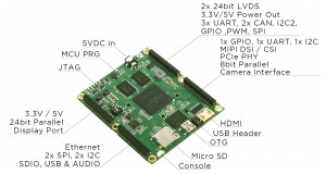
Habey has designed the Linux board around a Freescale i.MX6 processor based on ARM Cortex-A9 architecture. It runs an open source embedded Linux distribution with Yocto Project.

The industrial computer firm describes the HIO-EMB-1200 as a single-board computer with its own power input, on-board RAM, flash storage, HDMI, digital audio, USB ports and SD expansion.

The modular design gives eight 50-pin female headers on the top and bottom of the board for expansion modules.

Along with the base board, the company has developed a starter kit for power over Ethernet designs, and a development kit with LCD touch panel.

For more information on product availability go to Habey’s HIO Project website.

The Yocto embedded Linux images, support documents and source codes are also available at HIO Project’s wiki and GitHub.

Richard Wilson

ERNI to launch 100G ATCA connectors

ERNI to launch 100G ATCA connectors

ERNI to launch 100G ATCA connectors

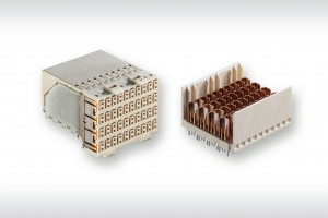
ERNI Electronics is to launch its ERmet ZDpro connector family for 100G ATCA systems next month.

This high-speed differential hard metric connector system enables data rates of >25 Gbit/s and claims to be the first connector system that meets the requirements for 100G ATCA technology.

The data rates and the improved transmission behaviour are mainly based on the reduced size of the signal termination, designed for vias with a diameter of only 0.30mm.

The drilling hole diameter for the shielding contacts is specified at 0.46mm. According to the company the fact that the reduction of the vias leads to an improved crosstalk behavior was the motivation to the further miniaturisation of the press-fit zone.

The communication technology shows an ongoing trend towards increasing data rates and higher bandwidths. This means there is a need for 100GbE (gigabit Ethernet) data transmission. Typical applications are the next generation of internet backbones, data centers or cloud computing.

ERmet ZDpro connectors fulfill the requirements and challenges of the interface between backplane and daughter cards in suchhigh speed systems, claims the company. The new product is based on the mechanical design of its ERmet ZD and ERmet ZDplus, with the same dimensions.

ERmet ZDpro connectors are backwards mating compatible to ERmet ZD and ZDplus connectors. This means that existing backplane designs do not need layout changes on the backplane side if customers want to upgrade their daughter cards in the first step before upgrading the whole system, although the layout on the daughter cards has to be modified, if ERmet ZDpro receptacles are used.

To benefit from the maximum performance of the ERmet ZDpro the company recommends backdrilling. Decreasing via stub length and the related “stub effect“ by backdrilling significantly reduces the reflections and the overall bit error rate of the connection.

The first products of the ERmet ZDpro family are the four-pair right-angle female connector and the related straight male connector with press-fit termination. Both will be available from September 2015.

The connectors provide 40 signal pairs. The male connectors are available with different contact lengths (3.8mm or 5.3mm). While the standard variants with 3.8mm contacts offer an optimised impedance behaviour the male connectors with 5.3mm contact lengths provide a 1.5mm higher wipe length of 2.9mm.

david manners

Three win Digi-Key/Silicon Labs IoT competition

The three winners of the "Your IoT Connected World" design contest have been announced

The three winners of the “Your IoT Connected World” design contest have been announced

Silicon Labs and Digi-Key have announced the three winners of the “Your IoT Connected World” design contest.

They are:

• Christian Klemetsson, who designed his “DeviceRadio” industrial automation solution to connect the real world to applications through virtual wires specifically within the industrial automation market. The goal of this product design is to deliver a custom IoT device on a solderless breadboard and controlled through the Internet in three minutes or less.

• Hoang Nhu, who developed a platform for extending the IoT through all parts of the home, from medication reminders to smart power plugs. The Apple HomeKit SmartHome and Wellness IoT Development Platform monitors home environments/energy consumption and daily activities to optimize home appliance settings as well as make recommendations and reminders for optimal wellness.

• Ekawahyu Susilo who developed “Snappy,” a modular robotics platform designed to help teachers engage students through science, technology, engineering and math (STEM) education. Snappy can be used for a variety of science project applications such as determining altitude with water bottle rockets, measuring collision impact in physics experiments, and building a simple local/Internet-connected weather station with humidity and temperature sensors.

Digi-Key supplied $10,000 worth of Silicon Labs components to each winner.

david manners

Microsoft ports border gateway protocol to Cavium XPliant switches

imageMicrosoft Azure Networking has ported its L3 Border Gateway Protocol (BGP) routing stack to Cavium XPliant switches.

This has been accomplished, the company says, through the use of the Switch Abstraction Interface (SAI), which enables portability and interoperability across different hardware platforms.

Historically switch silicon suppliers offered proprietary software interfaces requiring extensive software porting by customers to create an end user switch product. This resulted in a proprietary lock-in for these legacy switch silicon suppliers.

The SAI was defined as an abstraction interface for switching Asics to remove these barriers.

SAI enables system developers to port software to the best switch silicon that supports these SAI abstractions.

Earlier this year Cavium announced SAI support in the XPliant switch SDK (software development kit),  software now released for general use. Microsoft has easily ported Layer 3 BGP routing applications to the XPliant switch SDK based on the SAI interface.

“SAI adoption will enable customers to seamlessly deploy multiple vendors’ silicon into the network,” says Microsoft’s Kamala Subramaniam.

Cavium’s XPliant Ethernet switch family targets applications in cloud / enterprise data centers and service provider infrastructure, for both top-of-rack and backbone applications with bandwidths up to 3.2 Terabits per second in monolithic silicon support 1G, 10G, 25G, 40G, 50G and 100G interfaces.

This family of switches will also provide connectivity solutions for embedded applications.

david manners