Research is indicating there will be a completely new radio technology for the 5G mobile communications standard expected to hit the market by 2020.
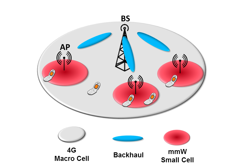
MiWaveS 5G network concept
Research work in the UK and across Europe into the next generation mobile phone standard is now focusing on the use of millimetre wave radio transmission at very high 30-300GHz frequencies.
If implemented, this will represent the biggest technology change for a mobile generation since the switch from analogue to digital GSM technology more than a decade ago.
For researchers in the UK, France and Germany everything is up for grabs. The standards work for the radio access network (RAN) has yet to begin.
The first discussions on potential global standards will start next month at a 3GPP standards meeting in Arizona.
According to Professor Rahim Tafazolli, director of the 5G Innovation Centre (5GIC) at the University of Surrey:
“Global 5G research is still taking place in isolation, but this will change. Various groups have different technology favourites, and the 3GPP standardisation discussions will start in September. I expect technology selection will start in 2016.”
The use of the millimetre wave frequency band, which is 30-300GHz, has benefits of spectrum efficiency, the use of lower power radio cells and data capacity, but will have significant implications for chipset makers.
In particular, the general switch from CMOS to gallium arsenide and gallium nitride process technologies.
The other reason for the radical jump in frequency is the lack of sufficient spectrum below 6GHz, which leads to high interference levels.
According to Dr. Laurent Dussopt from CEA-Leti and manager of the European Commission-funded MiWaveS project, the use of the millimetre wave frequency bands at 60GHz and 71-86GHz will enable data transmissions up to 10Gbit/s for backhaul and 5Gbit/s for mobile user access.
However, Dussopt believes this will be a challenge for the system architecture, networking functions and algorithms, radio and antenna technologies.
Millimetre wave radios use much higher carrier frequencies than 4G or Wi-Fi, allowing higher data rates, which could be as much as 50 times faster than 2.4GHz Wi-Fi. And at 60GHz there is significantly more unallocated spectrum.
According to researchers at The University of Bristol, which is also working on millimetre wave technology, the challenge at 60GHz is how to overcome the additional signal losses. If transmit powers and antenna gains were equal, at 60GHz the received signal would be 1000x weaker than a Wi-Fi signal.
Nokia’s Networks division is working with National Instruments to demonstrate the viability of high-frequency millimetre wave transmission for 5G.
“Our experimental 5G Proof-of-Concept system will be implemented using NI’s LabVIEW and PXI baseband modules, which is the state-of-art experimental system for rapid prototyping of 5G air interface available today,” said Lauri Oksanen, vice-president of research and technology at Nokia.
Aspects of the next generation mobile communications technology the companies are researching are peak data rates and cell-edge rates in excess of 10Gbit/s and 100Mbit/s, respectively.
Work in the European MiWaveS project is intended to demonstrate how low-cost or advanced millimetre wave technologies can provide multiGigabits per second access to mobile users and contribute to sustain the traffic growth.
It believes the exploitation of the available millimetre wave spectrum will be a key element in building high-throughput and low latency infrastructures for next generation heterogeneous mobile networks.
The UK’s main 5G research centre, the 5GIC at the University of Surrey is to be part of the MiWave S project.
Other project members include: CEA-Leti, Orange, Nokia, Intel, National Instruments Dresden and STMicroelectronics.
")