Synopsys tunes ARC EM processors for low latency apps

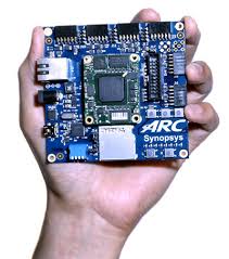
Synopsys has added to its processor IP offering with new ARC EM processors with an enhanced instruction set architecture that combines RISC and DSP processing with support for an XY memory system.

Synopsys tunes ARC EM processors for low latency apps

Synopsys tunes ARC EM processors for low latency apps

The EM9D and EM11D processor cores benefit from being able to retrieve instructions and data from memories that are tightly coupled to the processor pipeline. This can reduce the number of accesses to system memory which improves latency.

The ARC MetaWare development tool now offers full C/C++ programming support for the cores’ DSP instructions and XY memory as well as a library of DSP functions.

The toolkit also includes an ITU-T base-ops library for developing voice codecs.

These include FFT and DCT, FIR and IIR filters, as well as vector and matrix math functions.

Likely applications may include speech recognition and audio processing.

EM DSP cores implement a three stage pipeline. These new cores integrate separate X and Y memories with hardware support for address generation and DMA to move data in and out of the memories.

This enables a sustained throughput of one 32×32 MAC operation or two 16×16 MAC operations per clock cycle with minimal energy and area overhead.

These new processors also support full integer, fractional divide and square root operations, unaligned loads/stores and bitstream parsing.

These features enable the EM9D and EM11D to deliver the additional DSP performance required to execute complex sensor algorithms, as well as improve processing efficiency for a range of audio formats including MP3, SBC, OPUS and AAC LC.



Richard Wilson

Synopsys tunes ARC EM processors for low latency apps

Synopsys has added to its processor IP offering with new ARC EM processors with an enhanced instruction set architecture that combines RISC and DSP processing with support for an XY memory system.

imgresThe EM9D and EM11D processor cores benefit from being able to retrieve instructions and data from memories that are tightly coupled to the processor pipeline. This can reduce the number of accesses to system memory which improves latency.

The ARC MetaWare development tool now offers full C/C++ programming support for the cores’ DSP instructions and XY memory as well as a library of DSP functions.

The toolkit also includes an ITU-T base-ops library for developing voice codecs.

These include FFT and DCT, FIR and IIR filters, as well as vector and matrix math functions.

Likely applications may include speech recognition and audio processing.

EM DSP cores implement a three stage pipeline. These new cores integrate separate X and Y memories with hardware support for address generation and DMA to move data in and out of the memories.

This enables a sustained throughput of one 32×32 MAC operation or two 16×16 MAC operations per clock cycle with minimal energy and area overhead.

These new processors also support full integer, fractional divide and square root operations, unaligned loads/stores and bitstream parsing.

These features enable the EM9D and EM11D to deliver the additional DSP performance required to execute complex sensor algorithms, as well as improve processing efficiency for a range of audio formats including MP3, SBC, OPUS and AAC LC.


Richard Wilson

Synopsys tunes ARC EM processors for low latency apps

Synopsys has added to its processor IP offering with new ARC EM processors with an enhanced instruction set architecture that combines RISC and DSP processing with support for an XY memory system.

imgresThe EM9D and EM11D processor cores benefit from being able to retrieve instructions and data from memories that are tightly coupled to the processor pipeline. This can reduce the number of accesses to system memory which improves latency.

The ARC MetaWare development tool now offers full C/C++ programming support for the cores’ DSP instructions and XY memory as well as a library of DSP functions.

The toolkit also includes an ITU-T base-ops library for developing voice codecs.

These include FFT and DCT, FIR and IIR filters, as well as vector and matrix math functions.


Likely applications may include speech recognition and audio processing.

EM DSP cores implement a three stage pipeline. These new cores integrate separate X and Y memories with hardware support for address generation and DMA to move data in and out of the memories.

This enables a sustained throughput of one 32×32 MAC operation or two 16×16 MAC operations per clock cycle with minimal energy and area overhead.

These new processors also support full integer, fractional divide and square root operations, unaligned loads/stores and bitstream parsing.

These features enable the EM9D and EM11D to deliver the additional DSP performance required to execute complex sensor algorithms, as well as improve processing efficiency for a range of audio formats including MP3, SBC, OPUS and AAC LC.


Richard Wilson

Intersil buys Great Wall

Intersil buys Great Wall

Intersil buys Great Wall

Intersil has bought Arizona mosfet specialist Great Wall Semiconductor (GWS) for $19 million. A further $4 million is payable if performance metrics are met.

GWS was founded in 2002, has 10 employees and 22 patents related to lateral low-voltage power mosfet technology which allows low-gate charge power mosfets to be made on a CMOS process.

‘GWS’s design team brings valuable experience leveraging advanced design and process technology to enable power efficiency gains and footprint reduction in complex power systems,’ says Intersil.

“This small but experienced team will be a great asset as we continue to expand our power management capabilities,” says Intersil’s Mark Downing.

“GWS has differentiated itself through expertise in lateral power mosfet device and processing technology combined with miniature chipscale packaging,“ says Sam Anderson, CEO of GWS, “we have developed important intellectual property that enables energy savings and environmental progress.”

The basics of the firm’s technology is described in this lateral mosfet conference paper from APEC.

david manners

Intersil buys Great Wall

Intersil buys Great Wall

Intersil buys Great Wall

Intersil has bought Arizona mosfet specialist Great Wall Semiconductor (GWS) for $19 million. A further $4 million is payable if performance metrics are met.

GWS was founded in 2002, has 10 employees and 22 patents related to lateral low-voltage power mosfet technology which allows low-gate charge power mosfets to be made on a CMOS process.

‘GWS’s design team brings valuable experience leveraging advanced design and process technology to enable power efficiency gains and footprint reduction in complex power systems,’ says Intersil.

“This small but experienced team will be a great asset as we continue to expand our power management capabilities,” says Intersil’s Mark Downing.

“GWS has differentiated itself through expertise in lateral power mosfet device and processing technology combined with miniature chipscale packaging,“ says Sam Anderson, CEO of GWS, “we have developed important intellectual property that enables energy savings and environmental progress.”

The basics of the firm’s technology is described in this lateral mosfet conference paper from APEC.

david manners

Intersil buys Great Wall

wallIntersil has bought Arizona MOSFET specialist Great Wall Semiconductor (GWS) for $19 million. A further $4 million is payable if performance metrics are met.

GWS was founded in 2002, has 10 employees and 22 patents related to lateral low voltage power MOSFET technology.

‘GWS’s design team brings valuable experience leveraging advanced design and process technology to enable power efficiency gains and footprint reduction in complex power systems,’ says Intersil.

“This small but experienced team will be a great asset as we continue to expand our power management capabilities,” says Intersil’s Mark Downing.

“GWS has differentiated itself through expertise in Lateral Power MOSFET device and processing technology combined with miniature chipscale packaging,“ says Sam Anderson, CEO of GWS, “we have developed important intellectual property that enables energy savings and environmental progress.”
.

david manners

High speed stacked memory arrives with HBM standard

A stacked memory device which has the potential to achieve memory access speeds 14 times faster than today’s DDR4 has been demonstrated by eSilicon, Northwest Logic and SK Hynix.

High speed stacked memory arrives with HBM standard

High speed stacked memory arrives with HBM standard

The stacked memory device is complaint with the JEDEC 2.5D packaging standard known as high bandwidth memory (HBM).

The chip uses an FPGA-based controller core and PHY for the HBM standard architecture implemented in a Hynix memory array.

eSilicon packaged the FPGA controller designed by Northwest Logic and HBM devices on an organic interposer.

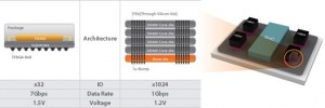
First-generation HBM devices provide eight channels of 128-bit data running at one Gbit/s/pin for a total system throughput of 128Gbyte/s.

According to the companies, they say second-generation HBM devices double the throughput.

They claim this is approximately 14 times the throughput available from a DDR4 DIMM running at 2,600 Mbits/pin. HBM has both power and cost advantages over competing technologies.

Bill Isaacson, senior director, product marketing at eSilicon, writes:

“HBM and system-in-package technology hold great promise to break the power and performance bottlenecks designers are currently facing with regard to memory subsystems.

“This joint effort with Northwest Logic and SK Hynix validates that HBM is ready to enter mainstream use.”

The HBM Controller Core supports both Gen 2 (2 Gbit/s/pin) and Gen 1 (1 Gbit/s/pin).

Brian Daellenbach, president of Northwest Logic, expects to see increasing interest in HBM applications.


Richard Wilson

High speed stacked memory arrives with HBM standard

A stacked memory device which has the potential to achieve memory access speeds 14 times faster than today’s DDR4 has been demonstrated by eSilicon, Northwest Logic and SK Hynix.

proGraphic3The stacked memory device is complaint with the JEDEC 2.5D packaging standard known as high bandwidth memory (HBM).

The chip uses an FPGA-based controller core and PHY for the HBM standard architecture implemented in a Hynix memory array.

eSilicon packaged the FPGA controller designed by Northwest Logic and HBM devices on an organic interposer.

First-generation HBM devices provide eight channels of 128-bit data running at one Gbit/s/pin for a total system throughput of 128Gbyte/s.

According to the companies, they say second-generation HBM devices double the throughput.

They claim this is approximately 14 times the throughput available from a DDR4 DIMM running at 2,600 Mbits/pin. HBM has both power and cost advantages over competing technologies.

Bill Isaacson, senior director, product marketing at eSilicon, writes:

“HBM and system-in-package technology hold great promise to break the power and performance bottlenecks designers are currently facing with regard to memory subsystems.

“This joint effort with Northwest Logic and SK Hynix validates that HBM is ready to enter mainstream use.”

The HBM Controller Core supports both Gen 2 (2 Gbit/s/pin) and Gen 1 (1 Gbit/s/pin).

Brian Daellenbach, president of Northwest Logic, expects to see increasing interest in HBM applications.


Richard Wilson