Surrey Satellites show 1m res imagery

The first 1m high resolution optical satellite imagery from the DMC3/TripleSat Constellation satellites is demonstrated today by Surrey Satellites Technology (SSTL) following the launch of three Earth Observation mini-satellites on an Indian PSLV in July.

The very high resolution imager on board the satellites provides 1m native ground sampling distance (GSD) in panchromatic mode and 4-metre GSD in multispectral mode with a swath width of 24km.

This 1m resolution pan-sharpened image taken on 2 August 2105 shows the Olympic Stadium in Athens, Greece.image

Sir Martin Sweeting, SSTL’s founder and chief executive, welcomed a comment from Dave Parker, chief executive of the UK Space Agency, who said: “Congratulations to SSTL on the acquisition of these 1m resolution images of our planet from the DMC3 constellation – a real demonstration of technical precision. SSTL’s expertise in small satellites plays a major role in the space sector’s £3.6bn contribution to the UK economy through exports.”

The Twenty First Century Aerospace Technology Company Ltd (21AT), a commercial Earth observation satellite operator based in Beijing, has bought all the imaging capacity of the three satellites for seven years to provide their satellite data services from the TripleSat Constellation. 21AT says it will also create new applications for customers and business opportunities for its worldwide partners through its operational information services powered by the TripleSat Constellation.

The wide swath width of the imagers, combined with agile off-pointing, will enable the TripleSat Constellation to target anywhere on Earth at least once per day and provides the best combination of spatial resolution and time resolution – aiming at stimulating operational monitoring applications, such as urban planning and intelligent management, based on changes detected by timely regular, cloud-free, very high-resolution imagery.

The DMC3 satellites were placed into a 651km sun-synchronous low Earth orbit by a PSLV-XL launch vehicle from the Satish Dhawan Space Centre, Sriharikota launch site in India on 10 July 2015. The launch was provided by Antrix and the Indian Space Research Organisation (ISRO).

The satellites in the TripleSat Constellation are phased 120° apart around the same orbit using their on-board propulsion systems. 21AT has contracted SSTL to provide satellite platform services for the Constellation in orbit.

The constellation satellites use the 450kg SSTL-300S1 series platform, which provides 45° fast slew off-pointing and is capable of acquiring multiple targets in one pass using multiple viewing modes.

SSTL has already manufactured a fourth SSTL-S1 Earth Observation satellite for another customer and has a production line ready to deliver further satellites of this type. Subject to agreement with 21AT, future satellites may have the opportunity to join the TripleSat Constellation.

david manners

ST creates ecosystem for STM32L4 ARM Cortex-M4 MCUs

STMicroelectronics has created a design ecosystem with development boards and software for its STM32L4 microcontrollers.

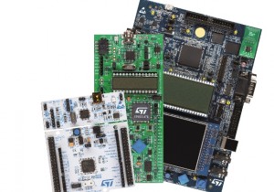
This includes a budget board for engineers, students, and hobbyists called STM32 Nucleo board (NUCLEO-L476RG) which costs $10.32.

PR_STM32L4

Three STM32L4 MCU development boards

The Nucleo board has Arduino Uno headers for adding shields and its own ST-Link debugger/programmer removes the need for a separate debug probe.

The STM32L4 MCU is notable for an 80MHz ARM Cortex-M4 core with DSP extensions and floating-point unit.

There is also a full spec Evaluation Board (STM32L476G-EVAL) priced at $289 and the $19.90 Discovery Kit (STM32L476G-DISCO) which incorporates a MEMS microphone and motion sensors, along with DAC, 96-segment LCD, and 16Mbyte QSPI flash memory.

The Discovery and Nucleo boards both provide direct access to mbed online tools.

Software support includes the STM32CubeMX configurator and initialization-code generator.

MCU-specific software provides a Hardware Abstraction Layer (HAL), application examples, and new Low-Layer APIs.

“The APIs can be used in parallel with the HAL and simplify migrating projects developed with STM32 standard peripheral libraries into the STM32Cube environment,” said the supplier.


Richard Wilson

Intelligent computers will work with humans

Prof Nick Jennings Soton

“If realised correctly, this vision of people and computational agents operating at a global scale offers tremendous potential” Jennings

A five year UK project has predicted the way humans will interact with intelligent computers.

“Instead of issuing instructions to passive machines, we will increasingly work in partnership with ‘agents': highly interconnected computational components that are able to act autonomously and intelligently, forming human-agent collectives [HACs],” said the University of Southampton, which lead the project, known as Orchid.

Agents can be in sensors collecting and analysing information to give the bigger picture of an emergency situation as it develops or in a smart meter monitoring the energy consumption in a home to recommend how occupiers might adapt to reduce energy cost and carbon footprint.
ORCHID Showcase: Re-inventing our relationship with computers

Its leader was Professor Nick Jennings, head of Southampton’s Agents Research Group.

Jennings said:

“It is simply unfeasible to expect individuals to be aware of the full range of potentially relevant possibilities and to be able to pull them together manually. Computers need to step up to the plate and proactively guide users’ interactions based on their preferences and constraints.

This shift is needed to cope with the volume, variety and pace of the information and services that are available.

In so doing, greater attention needs to be given to the balance of control between people and machines.

If realised correctly, this vision of people and computational agents operating at a global scale offers tremendous potential and will help us meet the societal challenges of sustainability, inclusion, and safety.”

Results are to be presented at the Royal Academy of Engineering in London later this month.

Examples on display will include:

Joulo
A home heating advice system that uses a temperature logger and on-line algorithms to provide feedback to households on how they are using their current heating system, along with autonomous intelligent home heating agents that learn the comfort preferences in order to provide efficient comfortable control.

AtomicOrchid
A mobile mixed-reality game in which first responders work with a response headquarters to rescue as many casualties as possible. “This game has allowed researchers to study team coordination and understand how human responders can be supported by computational agents that assist the planning and execution of the rescue mission, including the coordination of multi-UAV {drone] deployments,” said the University.

Japan Nuclear Crowd Map platform
Following Fukushima, citizen scientists deployed sensors and up-loaded data to help track the spread of airborne radioactive particles. To identify accurate information, the platform combines reports from thousands of sensors and uses machine learning algorithms to correct for biases and noise and weed out defective sensors.

Orchid was a £10m project (£5m from EPSRC, £5m from from project partners) with around 60 researchers from the universities of Southampton, Oxford and Nottingham, together with BAE Systems, Secure Meters UK, Rescue Global and the Australian Centre of Field Robotics.

The project has employed and trained 50 research fellows and PhD students, and generated over 200 publications, of which 40 are collaborations between the partners and half involve an international co-author.

“The Orchid legacy includes the development of 25 new academic collaborations and follow-on grants worth £15m. Orchid researchers have organised 25 major conferences and workshops and won over 20 prizes, awards and best papers,” said Southampton.

steve bush

Flex Logix adds RAM and DSP blocks to FPGA IP

imageFlex Logix is offering evaluation licences to SoC designers for block RAM and DSP cores which can be added to its embedded FPGA fabric.

Flex Logix’ technology allows system-on-chip SoC designers to embed field FPGA blocks, so allowing SoCs to be optimized or customized after the device is fabbed.

By adding block RAM and DSP, Flex Logix expands the tool kit available to designers for this post-production flexibility.

Applications such as encryption, networking and signal processing require blocks of RAM to be integrated into the FPGA to provide fast local memory to implement buffers, scratchpads, FIFOs, and other low-latency memory that improves performance.

While traditional FPGAs typically offer one type and size of RAM that can “emulate” different widths, Flex Logix’ Block RAM architecture can provide exactly the type and amount of memory an application requires.

This flexibility is accomplished by inserting block RAM between the logic cores—which “tile” together to make an array—controlling them with otherwise unused inward-facing inter-tile I/Os.

Flex Logix can support single-port RAM or dual-port RAM, any width, any amount; ECC, parity or no error checking; even MBIST—offering more flexibility than available in discrete FPGA chips.

In addition to local memory, many applications also require digital signal processing DSP capability. Wireless base station digital front ends, image and audio processing, and other applications require high-performance DSP functions such as Finite Impulse Response (FIR) filters, Infinite Impulse Response (IIR) filters, and Fast Fourier Transforms (FFT).

The basic building block for implementing these DSP functions is a pre-adder/multiplier/accumulator (MAC).

Flex Logix now offers an EFLX Logic core that incorporates 40 MACs with 22-bit inputs and 48-bit accumulation. The MACs can be combined for 2x precision and pipelined for high throughput. They can also be used as complex-number MACs for certain DSP algorithms.

Performance specs for a single Flex Logix’ DSP core are similar to that of existing stand-alone 28nm FPGA chips, achieving 500 Msamples/second for a 22-bit 5-tap FIR and 300 Msamples/second for a 22-bit 40-tap FIR. Multiple EFLX DSP cores can be combined to implement more complex DSP functions.

The EFLX Compiler maps standard Verilog/RTL into the EFLX array, including DSP and Block RAM (and even including external Block RAM if desired).

Customers do not require any FPGA expertise to use Flex Logix technology, says Flex Logix.

david manners

IoT gets a new wireless technology backed by Intel, Nokia and Ericsson

IoT has a new wireless technology and it has influential supporters in Intel, Nokia and Ericsson.

It is a narrowband version of 4G LTE, dubbed NB-LTE, which has been created just for the needs of the internet-connected devices and sensors which will make up the internet of things (IoT).

Nokia supports NB-LTE

Nokia supports NB-LTE

Not everyone supports the technology. Huawei of China is not a friend of NB-LTE and it believes there are better ways to adapt existing networks.

Unlike smartphones which require as large a bandwidth in the radio channel for downloading big data files such as video and music, IoT devices will only transmit small amounts of data.

But the main requirements of an IoT wireless protocol is that it must not require a big data processing function so the IoT devices can be low power and small.

The advantage NB-LTE has is that it will build on the proliferation of 4G LTE networks, requiring only an upgrade to existing infrastructure to support IoT services.

“Cellular networks already cover 90 percent of the world’s population so it makes sense to leverage this global footprint to support and drive IoT adoption through the standardisation of narrow-band LTE,”said Thomas Norén, head of radio product management, Ericsson.

Intel has said it will start offering first chips for narrow-band LTE in 2016.

The chip company will work with wireless network suppliers Nokia and Ericsson to support the upgrade of existing LTE networks with narrow-band LTE for the roll out of machine-to-machine communication and IoT services.

What other narrowband radio technologies could be used for IoT?

For short range wireless links mesh technologies such as Bluetooth and ZigBee will be used and even Wi-Fi extensions. But it may not be easy or even possible to scale these up for wide-area coverage.

“We believe in building an ecosystem around NB-LTE to speed up the take-up of the Internet of Things,” said Stephan Litjens, vice president, portfolio strategy & analytics, Nokia Networks.

Richard Wilson

TSMC uses Cadence design flow for 10nm finfet chip designs

TSMC has created a 10nm custom design reference flow for tools supplied by Cadence, and it is working on first commercial 10nm finfet chip designs.

TSMC uses Cadence design flow for 10nm finfet chip designs

TSMC uses Cadence design flow for 10nm finfet chip designs

The importance elements in the design of 10nm chips are: creating FinFET arrays which avoid density gradient effects and being able to handle multi-patterning designs.

The tools must also have the capability to extract and analyse real-time parasitics and electromagnetic violations during design implementation.

Cadence’s digital, custom/analogue and signoff tools have achieved certification from TSMC for V0.9 of its 10nm process and are expected to achieve V1.0 completion by Q4 2015.

The target for will be designing first 10nm smartphones and tablets application processors and high-end servers.

The Cadence tools in the flow include: Virtuoso custom IC advanced-node platform, Spectre simulation tool, physical verification software, Innovus, Quantus and Tempus timing signoff.

Dr. Chi-Ping Hsu, senior vice president and chief strategy officer for EDA at Cadence said: “We are now actively working with customers on 10nm designs and seeing great successes.”

According to Suk Lee, TSMC senior director, design infrastructure marketing division, the reference flows in both digital and custom design can “help customers reduce iterations and improve predictability while bringing their products to the market.”

See alsoImec and Synopsys work on 10nm finfet chip design


Richard Wilson

Bluetooth Europe 2015: Bluetooth Smart for IPv6 in the IoT

Internet of Things - IoT

Internet of Things – IoT

The Bluetooth Europe 2015 conference running in London today and yesterday, included a keynote from Nordic Semiconductor considering one possible realisation of the future dream of the Internet of Things (IoT), involving IPv6.

Entitled ‘Bluetooth Smart Sensor Networks over IPv6: Powering the IoT Market’ it envisaged Bluetooth Smart serving as the data-link layer for IPv6.

Thomas Bonnerud, Director of Product Marketing at Nordic Semiconductor, outlined possible benefits of combining IPv6 with the low-cost, low-power wireless technology of Bluetooth Smart. That Bluetooth Smart, the low-energy version of Bluetooth common to everyone’s smartphone, will serve as the data link IPv6 running on top, as is already the common case with IPv4 and Wi-Fi, for example.

The why

Currently we in the “Internet of my things”, he said. We are connecting ‘my things’ with Bluetooth Smart. Mainly “my things” and mainly connecting by phone. At this point there is no need for IP.

He also noted that the fastest growing apps in Bluetooth Smart today are those that connect to cloud services.

But the whole IoT concept depends on the adoption and rollout of IPv6, he argued, and thus we have to assume IPv6 is going to happen albeit with a gradual phasing. He then talked about future requirements, giving an example of maintenance of equipment and machinery, such as the health status of freezer cabinets in a large supermarket or warehouse…

“These possible ‘Things around us’ are the next frontier for Bluetooth Smart. Non-personal, not tied to my phone, and with 24/7 connectivity potentially required. For example, a door lock.”

“Maybe the devices are part of a larger distributed network. There will be a desire to leverage existing infrastructure.”

This is where IPv6 over Bluetooth Smart provides a solution, he said

Bluetooth Smart routers, not gateways

He anticipated the increasing use of Bluetooth Smart routers, rather than gateways, as basic building blocks for larger networks. In other words multi-mode Wi-Fi, Ethernet and other protocol devices. He said they were “coming along now” this year, citing technologies such as BlueZ, the Linux-based Bluetooth stack, and OpenWrt, the Linux-based wireless router. He also flagged “6LoWPAN”, an acronym of IPv6 over Low power Wireless Personal Area Networks.

The barrier for adoption is alot lower than other technologies, he said.

Basically, “use proven IP technology, leveraging existing infrastructure” – in this case Bluetooth Smart. Things to services, and things to things, either in the local network or remotely.”

Note that the Nordic nRF51 IoT Software Development Kit, released at the end of last year, covers this area, extending IP addressing all the way to the ‘things’ in IoT. According to the company:

The first release of the protocol stack includes: Internet Protocol Support Profile (IPSP), 6LoWPAN adaption layer, IPv6 internet routing layer, User Datagram Protocol (UDP) and Transmission Control Protocol (TCP) transport layers, Constrained Application Protocol (CoAP), and Message Queuing Telemetry Transport (MQTT) application layers, plus a range of application examples. A compact memory footprint also means that the complete protocol stack can run on the nRF51 Series SoC in a single-chip configuration, enabling developers to minimize power, size, and cost of end products.

Common IP upper layers

This approach enables heterogeneous networks, using common IP upper layers, he said, removing the need for smart gateways. “It’s all IP on the top – an IP-based application layer, providing interoperability across the networks”.

“We need to align with the Internet. Why should IoT be any different? Why shouldn’t the “things” behave exactly like (Internet-based) servers today? It’s a proven solution: scalable, predicable and robust.

“It’s about not re-inventing the wheel.”

For security, he further cited DTLS/TLS (Datagram Transport Layer Security) for providing secure end-to-end comms – a way for applications to communicate which prevents eavesdropping or tampering. That the means of securing remote banking transactions could be used with Bluetooth Smart.

“It requires”, he admitted, “multiple vendors to support the concept.

Of course, it was pointed out that IPv6 is one of those technologies forever on the cusp of realisation, forever the bridesmaid in terms of real-world implementation.

His answer was a challenge to the whole premise of IoT, and the realisation of the tech industry’s latest golden horizon: maybe IPv6 has to happen if IoT is going to be real, with millions of extra, directly-addressable nodes; you can’t have an Internet of Things without it.

What are your thoughts? Leave a comment below.

For more on the Nordic nRF51 Series Bluetooth Smart SoCs and IPv6 see ‘Nordic Semiconductor IPv6 over Bluetooth Smart protocol stack for nRF51 Series SoCs enables small, low cost, ultra-low power Internet of Things applications

The Bluetooth Europe 2015 conference is organised by the Bluetooth SIG.

IPv6
Internet Protocol version 6 is the most recent version of the Internet Protocol (IP), providing an identification system for computers across the Internet.Using an 128-bit address system (eight groups of four hexadecimal digits) it crucially allows 2128 addresses. This is far more than the current, 32-bit address IPv4 system, which has faced address exhaustion.

Unfortunately IPv4 and IPv6 are not interoperable, which has slowed the latter’s introduction.

Alun Williams

MIPS core brings virtualisation to Microchip MCUs

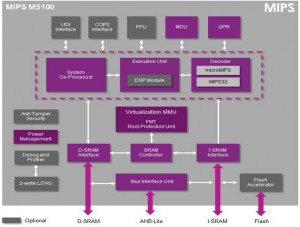
Microchip’s latest 32-bit microcontroller, the PIC32MZ, is an early implementation of the MIPS M5150 CPU.

Dubbed the Warrior M-class processor by Imagination, the company behind it, this is thought to be the only microcontroller-class CPU  to feature full hardware virtualisation.

This means it can be used to run multiple operating systems or applications on a single physical processor-based system.

A MIPS M5150 CPU can run up to seven guest operating systems in parallel, according to Imagination.

MIPS M5100

MIPS M5100

The Warrior M-class cores effectively compete with ARM’s Cortex-M series.

The cores are based on existing microAptive cores, with three added features: hardware virtualisation, a floating point unit, and anti-tamper.

According to MIPS business development manager Ian Anderton, performance is 1.57Dmips/MHz and 3.44CoreMark/MHz, emphasising that this is running compact code, not expanded code using ‘in-lining’ to boost benchmark performance.

Virtualisation allows a core to run multiple operating systems, time-sliced onto the core without them having any knowledge of each other. In this case, it is full hardware virtualisation, so operating systems run with “no software modification required”, said Anderton. Any mixture of up to seven ‘guests’ (operating systems, apps, kernels, schedulers or supervisors) can run.

“If one crashes, the others do not,” said Anderton, allowing a Linux user interface to run alongside control software without endangering the control function. Virtualisation also prevents the hacking of one application through another.

The Imagination blog gives an example application with the new 32-bit Microchip MCU used in a smart home hub:

“A MIPS M-class CPU inside a smart home hub can place door and window locks in separate virtualized containers to avoid compromised security throughout the home. Also a separate container can handle lighting control or the connectivity stack; any change in the operation of a container would not affect the others.”

You can see this demonstrated in a video with a MIPS-based development board when the Linux-based operating system running in one virtualized container restarts, the second container controlling the motor operation continues running.


Richard Wilson

ECCE: 650V GaN transistor hits 100A for solar

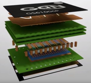
GaN Systems GS61006P package.jpg

Packaging the earlier GS61006P

GaN Systems is showing a 650V 100A GaN transistor at the IEEE Energy Conversion Congress & Expo in Montreal.

Sampling with potential solar, industrial and automotive customers, GS66540C  can switch faster than 100V/nS, claims the Canadian firm. Rds looks to be around 20mΩ

Packaging it describer as “an evolved form” of the firm’s bond-wire-less laminate-based GaNPX packaging, specially developed for higher operating currents, with lower inductance and improved surface mount mechanical robustness required – the latter aimed at industrial and automotive markets.

Further details do not appear to be available yet. The majority of the firm’s high power transistors need 6V gate drive with no requirement for negative voltages in the off state. Gate resistors are needed to control the fast turn-off and prevent gate voltage transients from occurring through the drain-gate capacitance. 

The body of existing GaNPX packaging is constructed from FR-4-like laminate and has an isolated heat tab (to which the die is directly bonded), which must be electrically connected externally to the source for proper operation.

Also at ECCE’ there will be a 2kW commercial vehicle inverter from with GaN System’s transistors from Ricardo and a 3kW, 800-380V bi-directional dc-dc converter for home use from US consortium NextHome.

ECCE’15 is in Montreal over 20-24 September.

steve bush

Manchester researches 3D printed graphene ink batteries

Batteries could one day be 3D-printed on the desktop using graphene ink, say researchers in Manchester.

Manchester researches 3D printed graphene ink batteries

Manchester researches 3D printed graphene ink batteries

A government-funded project at Manchester Metropolitan University wants to use the city’s pioneering expertise in graphene technology to develop a desktop printer which will be used to create batteries and supercapacitors that could be used for energy storage in devices from solar power generators to smartphones.

Professor Craig Banks, associate dean for research and professor in electrochemical and nanotechnology, who is leading the research project, believes the use of graphene ink in 3D structures should increase the charge storage capacity of batteries.

 “This project will be utilising the reported benefits of graphene, which is more conductive than metal, and applying these into energy storage systems,” said Banks.

But is it the combination of graphene with 3D-printed structures which is the interesting part of this project.

“The architecture of energy storage systems can be improved through the use of 3D structures, which have high surface areas, good electrical properties and hierarchical pore structures/porous channels,” said Banks.

“We’re trying to achieve a conductive ink that blends the fantastic properties of graphene with the ease of use of 3D printing to be manipulated into a structure that’s beneficial for batteries and supercapacitors.”

Researchers are analysing new techniques for rapid 3D printing with conductive graphene ink to create the batteries, funded by £500,000 from the EPSRC.

They want to improve on existing techniques which use ‘semi-graphene’ inks that contain graphene but also carbon black and graphite, which can reduce the material’s performance.

The process of 3D printing also needs to be refined as each layer that is printed has to be cured an hour before another layer can applied.

According to Banks, the research needs to figure out a way to cure it directly, possibly by shining a UV light on to it, as anything above a micron level takes a long time.

“Ideally, we could have the brilliant scenario where you just plug in and go – printing whatever structure you want out of graphene from a machine on your desk,” said Banks.

Graphene, which has exceptional electrical and thermal conduction properties, was discovered at the University of Manchester in 2004.


Richard Wilson