Five million Raspberry Pi’s is a Sony UK success story

Five million Raspberry Pis have been manufactured by Sony UK Technology Centre in Wales since the educational computer was launched three years ago.

Five million Raspberry Pi's is a Sony UK success story

Five million Raspberry Pi’s is a Sony UK success story

During the three year relationship the site has made five different models of the Pi, has increased its production from 10,000 units per week to 80,000 units.

“The Raspberry Pi, is a fantastic example of UK innovation, design and engineering, at its best,” said Steve Dalton OBE, managing director of Sony UK Technology Centre.

Sony has also resulted in the employment of 70 new staff  and 30 more will be recruited by the end of the year.

Eben Upton, Co-Founder of The Raspberry Pi said:

“Raspberry Pi is a British product, created by British engineers, that has found a huge global market.  South Wales has a long tradition of manufacturing, and we are very pleased that the success of Raspberry Pi has secured new, skilled jobs in the area. Global success can be transformative within local communities, and we’re proud to be part of that here in Pencoed.”

The product which has been developed by non-profit Raspberry Pi Foundation, is designed to stimulate young people’s interest in computer programming and electronics, but it has been hugely popular with hobbyists and developers.

Pencoed-based Sony UKTEC is producing the Raspberry Pi for the its two distributors, element14 and RS Components.

Claire Doyle, Global Head of Raspberry Pi at element14, said:

“We’re delighted to have been able to make such a success of the Raspberry Pi’s UK manufacture.  Working with Sony’s UK Technology Centre team in Pencoed has been an easy decision from the start. By making Raspberry Pi in Wales we’re able to ensure great quality and exceptionally competitive pricing, and have been able to benefit from a really great business relationship.”

To celebrate the milestone, Sony UKTEC welcomed Jo Johnston MP, Minister of State for Universities and Science for UK Government, Jonathan Hardie, Global Head of Manufacturing from leading manufacturer and distributor element14 and Phillip Colligan and Eben Upton from the Raspberry Pi Foundation.

See alsoVideo -How they make Raspberry Pi in the UK

Richard Wilson

UK firm harvest ambient RF for IoT

Drayson FreevoltAmbient RF signals are a viable source of energy, claims UK-based Drayson Technologies, which has patented a technique to harvest them.

Branded Freevolt, it uses an antenna, ‘non-linear device’, RF filter and a power manager (PMM in diagram).

“To integrate Freevolt into different devices, Drayson Technologies has developed standard harvesters but can also provide different antenna and rectifier designs, depending on the application requirements,” said the firm, adding: it is important to note that a harvesting antenna can have different and unique characteristics depending on the application.

It gives the example of a device placed on a wall, where the antenna can be optimised to cover a broad angle and have the appropriate polarisation and frequency bands to take advantage of the maximum number of existing RF sources.

Drayson efficacyIn a white paper, the firm predicts efficacy, and describes ambient field measurement results that yielded 600-700nW/cm2 peak in a office block from Wi-Fi, GSM and 4G LTE, and a peak of 6.7uW/cm2 from 3G signals in busy outdoor London locations.

Drayson is marketing a UK-made RF-powered air quality sensor tag called CleanSpace. “This technology creates a crowd-sourced network of personal air sensors, initially across the UK and then expanding to major cities across the world, which will all be powered by Freevolt,” said the firm.

steve bush

AMD unveils PRO A-Series desktop and mobile processors

HP EliteDesk 705, with AMD PRO A-Series desktop processor

HP EliteDesk 705, with AMD PRO A-Series desktop processor

AMD has introduced its most powerful line of AMD PRO A-Series mobile and desktop processors.

Formerly called Carrizo and Godavari PRO, the processors are intended to run Windows 10, said AMD.

PRO A-Series Mobile 

These have the firm’s fastest mobile processor – version A12 running at up to 3.4GHz. There are 12 cores (4 CPU + 8 GPU).

Graphics are Radeon R7, with up to 800MHz clocking and 512 graphics compute cores. “It is the first commercial processor in the industry designed to be compliant with the Heterogeneous Systems Architecture [HSA] 1.0,” said AMD.

The device is ARM TrustZone hypervisor capable, enabling TrustZone to run on the on-board secure processor, and it has a HEVC (High-Efficiency Video Compression) decoder for streaming HD content.

The chips are already available in some HP EliteBook laptops.

PRO A-Series Desktop

“With support for Quick Stream PRO, the new AMD PRO desktop processors virtually eliminate the lag in latency-sensitive applications like VoIP and streaming video.,” said AMD, “Quick Stream PRO uses built-in intelligence to identify and allot more bandwidth for businesses’ highest priority applications.”

The chips are already installed some Lenovo M79 Towers and HP EliteDesk 705 Micro Towers.


steve bush

Wristband heart rate sensor includes DSP

AMS AS7000 in action - a wristband heart rate sensor

AMS AS7000 in action – a wristband heart rate sensor

AMS has launched an optical heart rate sensor for wrist wearables.

Called AS7000, it measures heart rate by shining light into blood vessels, which expand and contract as blood pulses through them, and analysing scattered reflections – which is called photoplethysmography (PPG).

In a 6.1 x 4.1 x 1mm package, the device include two green LEDs and a photo-sensing signal processing IC – based around an ARM Cortex-M0. Green is chosen to best-sense pulse, and transducer spacing makes it most sensitive to scattering from an appropriate depth.

Although barriers in the package block light travelling direct from LEDs to photodiodes, said AMS, reflected pulse information is only a ~1% ripple on top of dc returns and large perturbations from movement.

“Unlike existing optical analogue front-ends which produce raw PPG readings, AS7000 integrates a digital processor which converts PPG readings into digital heart rate and heart rate variation”, claimed the firm.

AMS AS7000 photoTo work properly. the module has to be paired with an external accelerometer. This allows internal algorithms to filter-out the motion artefacts. “This means that the module can maintain high accuracy whether the user is resting or exercising.” said AMS.

The module also enables skin temperature and skin resistivity measurements through interfaces to and external thermistor and two skin electrodes.

Alongside the module, AMS is offering opto-mechanical design-in support which provides OEMs with electrical, mechanical and optical design guidelines to simplify optical design considerations such as air gap and glass thickness, and the design and material of the wrist strap and housing.

A wristband demonstration kit is available, which uploads readings via a Bluetooth interface board to an Android phone or tablet. An app presents results and allows real-time logging.

AMS has compared the demo kit to a traditional chest band sports heartrate sensor (Plolar RC3GPS) and claims close agreement.

AMS AS7000 app circuit

Application. Only green LEDs implemented in AS7000AA

AS7000AA AS7020 AS7024
MCU ARM Cortex M0 no no
memory 32k rom
4k ram
128byte FIFO 128byte FIFO
Analogue front ends 2 2 2
skin temp + resistance yes yes yes
ECG amplifiers no yes yes
LEDs green + green red + infra-red green + IR, green
Dimensions
mm (target)
6.1 x 4.1 x 1
20pin
0.4mm pitch
5 x 2.7 x 1
18pin
0.4mm pitch
6.1 x 2.7 x 1
20pin
0.4mm pitch
samples available available Nov. 2015
c-samples available Jan 2016 Feb/Mar 2016
Focus application Simple wristband phone Smart band / watch


steve bush

ST digital division faces guillotine

The French business weekly magazine Challenges reports that the future of ST’s digital division is now in the hands of President Francois Hollande.image

The French Economics Minister and the Defence Minister have reviewed the possible divestment or closure of Crolles, the Finance Ministry has had its say, the CFE-CGC union has been to see Hollande’s advisers and now the decision on what to do rests with the President.

The magazine reports that ST CEO Carlo Bozotti is accused, in a report by the Direction générale des entreprises (DGE) de Bercy, of sabotaging the digital division by publicly referring to its “unacceptable losses” – remarks which are alleged to have caused customers to freeze contracts, so further weakening the division and adding to the justification for closing it.

At stake are 2,500 jobs at Crolles and the last vestige of European-controlled access to advanced semiconductor production.

There are various proposed scenarios – sale or closure of the entire site involving 2,500 jobs, a reduction in jobs by between 1,000 and 1,200 people, or a reduction to a rump of only 300.

However there are warnings that a big hit at Crolles could affect another 20,000 jobs in the Grenoble region.

ST management is criticised for “supporting the share price at the expense of investment planning for the future.” ST is said to have spent $2.6 billion on dividends between 2005 and 2014 while the company has made losses of $3.6 billion. Last year it paid out $354 million to shareholders while losing $465 million.

Arguments for keeping Crolles going are the importance of the military not having to rely on American components and the opportunity presented by FD-SOI for providing leadership in IoT and connected cars.

France and Italy have 27.5% stakes in ST but waived their dividends to provide resources for investment. Italian government sources are staying schtum on the issue of the digital division.

david manners

FTDI Chip boosts EVE ecosystem

FTDI Chip has enlarged the development ecosystem surrounding its Embedded Video Engine (EVE) platform for advanced human machine interface (HMI) implementation.

The latest additions concern the FT810 series of high resolution EVE ICs, which are now in full scale production. In order to support these devices, the company has announced the VM810C50 family of compact development modules. They extend the functionality offered by the VM800C family that accompanies the FT800 series, so that large higher clarity imagery can be rendered and faster data transfer rates benefitted from.

The VM810C50A-D features a 5.0-inch TFT display with WVGA (800×480 pixel) resolution and a resistive touchscreen. Conversely, for the VM810C50A-N, the display is not included.

Instead, through use of its 40-pin FFC interface, a suitable 4.3/5.0-inch LCD (with SVGA, WVGA, VGA, WQVGA or QVGA resolutions and a 4-wire resistive touch screen interface) may be attached. This means that the appropriate display can be chosen and subsequently connected.

Both of these credit card sized units act as SPI slaves connecting to the specified system microcontroller through their single SPI interfaces.

They each have a built-in micro speaker, audio power amplifier, 3-stage audio filter, an audio line out option and LCD backlight control.

Power can be drawn for these modules via either the 2.0mm power jack, the USB Micro-B port or SPI interface. The SPI interface supports 5V tolerant buffers when using a 5V SPI supply.

The FT810 EVE devices from FTDI Chip combine touch, display and audio functionality on a single chip and employ the innovative approach to HMI implementation that has been pioneered by the company. Here images, templates, overlays, fonts and sounds are treated as objects.

Using this object-orientated methodology, graphics can be rendered line-by-line at 1/16th pixel resolution, as opposed to pixel-by-pixel.

This streamlines implementation, allowing marked reductions in cost, board real estate and system complexity. The FT810 and other members of the FT81x series are able to work with displays of up to 800×600 pixels.

They have 18-bit or 24-bit RGB interfacing options, plus 1Mbytes of RAM capacity for storing graphics data. A built-in JPEG decompression engine provides better graphics data usage and enables more effective HMI implementation.

These devices support multiple colour palettes of 16-bits and 32-bits with transparency. Their SPI interfaces support 30MHz operation.


david manners

Memsstar raises funding to boost exports

Memsstar, the Livingston manufacturer of MEMS manufacturing equipment has secured a imagesignificant funding deal with Santander supported by a guarantee from UK Export Finance.

Memsstar makes etch and deposition systems for MEMS manufacturing. It also represents SMEs in a range of European funding programmes.

Memsstar exports around 90% of its products and is looking to capitalise on this momentum in key markets.

The business currently has an annual turnover of circa £8 million but is targeting to grow this to £13 million over the next two years.

“This will provide the company with a source of working capital to enable the ongoing development of our customer base and ensure that we remain competitive for our existing customers,” says the company’s CFO Keith Rutter.

“This is a great example of how a government guarantee can work alongside a trade specialist bank to help a leading, innovative UK firm,” says Jonathan Leonard of UK Export Finance.

david manners

Failure should not be an option for Al capacitor

The aluminium capacitor is a common feature of power supplies, since it is the most suitable for functions such as energy storage and low- or high-frequency filtering. Unfortunately, aluminium capacitors are also often the components most prone to failure: the operating lifetime of an aluminium capacitor will tend to determine the operating lifetime of the entire power supply, writes Marcin Chelminski of Future Electronics.

This means that designers have to take great care when calculating the parameters of aluminium capacitors to choose the most appropriate part for their device.

The choice of capacitor also has to balance cost against performance: after magnetic components, aluminium capacitors are often the most expensive passive components in a power supply.

The reliability of an aluminium electrolytic capacitor is generally measured by its expected life in use.

Minor factors that affect their life include humidity, vibration and heat transmitted through the printed circuit board patterns.

But three other factors have a greater effect on useful life, these are: ambient temperature, ripple current and applied voltage.

The basic application guidelines for aluminium capacitors say that operating temperature, applied ripple current and applied voltage should always stay below the specified maximum allowable values.

But these guidelines do not provide enough information to enable power‑supply designers to optimise for long operating life.

For this, they need to estimate the effect on lifetime of variations in operating conditions within the maximum allowable limits.

By accurately estimating the effect of changes in operating conditions, designers can extend the lifetime of aluminium capacitors in any given application.

The latest generation of dedicated power-supply capacitors, which benefit from the most recent advances in design and materials, can offer long lifetimes of up to 15 years in a surprisingly wide range of operating conditions without incurring the cost ultra high reliability capacitors.

Aluminium capacitor failure modes

Aluminium capacitors implement a variety of functions, depending on their position in the circuit.

As an input buffer in an AC-DC converter, an aluminium capacitor provides energy when the mains input voltage is too low, or stores energy when it is too high.

As an output buffer, an aluminium capacitor performs filtering and acts as a current sink for an inductor.

In operation, these capacitors can fail in a number of ways:

  • catastrophic failure occurs when the capacitor completely breaks down, due to a short or open circuit.
  • degradation occurs when the capacitor continues to function, but its performance has deteriorated to some extent.

In the case of degradation, for instance, the device’s capacitance might fall over time. Whether the change in value is acceptable or not depends on the requirements of the application. If it is unacceptable, the device has effectively failed.

A short circuit between the electrodes can be caused mechanically, by shock, vibration or stress on the leads.

It can also be caused electrically, by the application of a pulse current or voltage which exceeds the rated maximum value.

There can be various causes of an open circuit. For instance, if the capacitor is subjected to too high a force at the time of mounting, the connection between the lead wire and the tab could be twisted or distorted.

High temperature is also dangerous, either by operating at a temperature above the rated maximum, or through exposure to excessive heat transmitted through the circuit board’s tracks, which vaporises the capacitor’s electrolyte.

Similarly, exposing the capacitor to excessive ripple current causes its internal temperature to rise, drying the electrolyte.

A fall in capacitance and increased power losses due to high equivalent series resistance (ESR) occur when:

• a reverse voltage is continuously applied

• the capacitor is subjected to a very high number of charge/discharge cycles

• applied current exceeds the maximum rated ripple current.

Optimise for conditions

Standard load life test limits applied to aluminium capacitors (at their rated voltage and maximum rated temperature) typically measure the elapsed time until the capacitor suffers a 20% or 30% decrease in capacitance from its initial value, a 200% or 300% increase in loss tangent (a measure of the power losses attributable to the dielectric), or a 200% increase in leakage current – whichever occurs first.

These standard limits provide a quick but rough means of comparing the performance of competing devices. But they do not necessarily reflect the requirements of any given application.

So to optimise the lifetime/cost trade-off and find the best possible capacitor for a specific power supply, the designer must calculate the expected life of capacitors under evaluation in the expected operating conditions of the application.

Before doing so, it is worthwhile considering how the operating conditions of the power supply might be modified so as to minimise the hazard to any aluminium capacitors on the board.

The electrical characteristics of aluminium electrolytic capacitors are more sensitive to temperature than those of other types of capacitors, because the properties of the liquid electrolyte in aluminium capacitors, (such as conductivity and viscosity) are strongly affected by temperature.

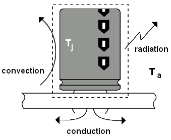
To reduce the device’s exposure to high temperatures, the designer needs to understand the flow of thermal energy through it (Figure 1).

Inside the dotted line, all the materials are at the device’s junction temperature (Tj); outside the dotted line is the ambient temperature (Ta).

The heat generated inside the dotted line is carried outside it by convection, radiation and conduction.

TAP1422_capacitors_Fig 1

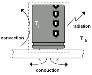
Figure 1: the three ways in which heat escapes from a power supply’s capacitor

If the designer can implement a means to improve the heat flow out of the capacitor, its expected operating lifetime will be extended.

Indeed, according to the Arrhenius theory, the life of an aluminium capacitor doubles with every 10°C fall in ambient temperature.

Such a fall has a direct effect on the designer’s lifetime calculation when the heat generated by resistive losses (for instance, in timing circuits) is negligible.

The basic method of cooling a capacitor is to mount it in free space. The natural circulation of air around the device will provide sufficient cooling for most applications.

If this is not enough, a heat sink will increase the flow of heat from the device. The most common type of heat sink is an aluminium extrusion attached to the closed end of the capacitor. An alternative is a semi-circular extrusion designed to clamp to the case of the capacitor.

Whichever capacitor is used in a power supply, the designer can ensure that the device survives for its average rated lifetime by regulating the temperature, ripple current and applied voltage to within the manufacturer’s specified limits.

Marcin Chelminski, central applications engineer, Future Electronics (Poland)


Richard Wilson

Plessey raises £30m to expand GaN-on-Si LED manufacturing

Plessey is to carry out a major expansion of the company’s LED manufacturing facility in Plymouth, after securing a £30 million loan from Deutsche Bank. image

The £60 million expansion will provide the base for new solid state lighting technologies and products, increasing the Company’s production capabilities by a factor of 30, more than tripling its workforce to about 535 employees and positioning Plessey to capture a significant share of the multi-billion dollar, and growing, solid state lighting market.

Plessey’s MaGIC GaN-on-Silicon technology can cut the cost of LED lighting by using standard silicon manufacturing techniques instead of sapphire-based manufacturing.

“Deutsche Bank is providing us with a senior secured term loan facility that meets our financial needs for the next three to five years,” says Plessey CFO Iain Silvester, “the bank has come up with a progressive flexible facility that supports our expansion plans for our manufacturing capacity here in Plymouth. Plessey will increase its manufacturing capacity from over 100 million square millimetres of Gallium Nitride material per year to more than 3 billion square millimetres. The facility modifications, which are also supported by £6.7 million from the Regional Growth Fund, will take place during 2015, with additional manufacturing tools and facilities coming on stream through the end of this year through to 2017. During this time we expect about 400 new jobs to be created.”

Michael LeGoff, Plessey’s CEO added: “We are entering a very exciting period for the company with our new technology and products now gaining traction in one of the fastest growing technology markets, solid state lighting. The expansion is highly significant for the Company but also for British high-tech manufacturing,” says Plessey CEO Michael LeGoff, “it aligns well with national strategies, such as the Growth Review, that support manufacturing and make the UK a global leading exporter of high value goods.”

david manners

Socionext in volume production of camera engine supporting new sensor functions

Socionext, the Fujitsu-Panasonic SoC jv, is in volume production of a camera front engine specialized for Bayer data processing that supports the latest sensors.socio

The MB86S29 is a Milbeaut Image Processor aimed at smartphones. By supporting the latest image sensors, the MB86S29 lets module makers implement these functions without replacing their application processors.

Recently, it is common to find cameras in smartphones or other mobile devices that are configured with application processors (AP) equipped with built-in image signal processor (ISP) functionalities. These APs can directly process output from image sensors, and help reduce the footprint and cost of camera modules.

The MB86S29 supports this trend as a “Camera Front Engine” that replaces conventional ISPs. Connected in between an image sensor and an AP, it is specialized for Bayer data processing, so users can configure their APs with the same interface directory connected to image sensors, and to make full use of phase detect auto focus (AF) or high dynamic range (HDR).

The MB86S29 has 4 lanes each of 2.1Gbps MIPI Rx / Tx. It can process 16M pixel images at 30 frame per second (fps). It is also applicable for noise reduction, shading correction, and 3A (AE / AF / AWB) detection. It is available in the smallest package of any member of the Milbeaut series, at 4mm x 4mm.

Since its first release in 2000, the Milbeaut series of image processors has established a track record in applications from digital SLR cameras for prosumers to commodities like smartphones, or industrial equipment like security cameras. Socionext will continue to deliver a broad range of imaging solutions, based on its technological expertise and a long history of providing services to its customers.

The MB86S29 has been designed to utilize “Hybrid AF”, which combines the accuracy of contrast AF and the speed of phase detect AF, enabling maximum 4x faster AF, in comparison with the previous Milbeaut products.

The MB86S29 also supports Sensor HDR. Conventional HDR imaging, which generates a picture from multiple frames taken with different exposures, has disadvantages, such as images blurs caused by the difference between the frames, and time needed to take those multiple frames. The MB86S29 can process data with different exposure settings within one image so it can process the HDR images with higher visibility in 16M pixel, at the speed of 30 fps.

□ MB86S29 Specifications
・ 16M Pixel at 30fps, Bayer Output
・ Compatible with phase detect AF Sensors
・ Compatible with Sensor HDR
・ Defective Pixel Correction (including pixels for phase detect AF)
・ Shading Correction
・ Package: 4mm x 4mm
・ MIPI-Rx: 4 lanes (2.1Gbps) + 2 lanes (1.5Gbps)
・ MIPI-Tx: 4 lans (2.1Gbps)
・ Dual ARM processor Core

TheMB86S29 costs $3 when purchased in volume quantities of 5 Million pieces or more.

david manners