Author Archives: steve bush

3D printing novel optical fibres

Soton Zepler fibre towerResearchers at the University of Southampton will attempt to make novel optical fibres using 3D printing.

To make glass optical fibres, a block of glass called a ‘pre-form’ is heated close to melting point and pulled so that it gets longer and thinner – a process called ‘drawing’.

The fibre inherits characteristics from the pre-form, so for a traditional fibre the preform starts as a cylinder of glass with a high refractive index core along its centre.

Southampton is a world leader in advanced fibres which have complex features – doping profiles and voids running their length, for example.

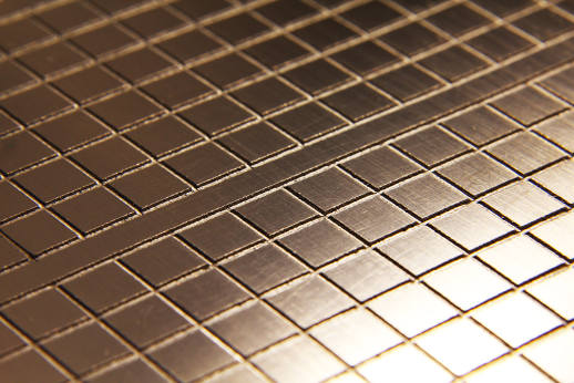
The latest are ‘microstructured’ fibres, where fibres with a certain internal structure are precisely stacked into a bundle, and then the bundle is drawn, and the process perhaps repeated, to produce a fibre fractal-like complexity – it is this process that was used to produce the microstructured ‘microchannnel plates’ used in second-generation image intensifiers.

Photonic bandgap fibre, for example, is a type of microstructured fibre which is hotly anticipated by the telecoms and datacoms industries, said the University, and 3D-printing might allow micro-structured pre-forms to be made in one step.

“We will design, fabricate and employ novel ‘multiple materials additive manufacturing’ [MMAM – 3D printing] equipment to enable us to make optical fibre preforms in silica and other host glass materials,” said Professor Jayanta Sahu of the University of Southampton’s Zepler Institute. “Our proposed process can be utilised to produce complex preforms, which are otherwise too difficult, too time-consuming or currently impossible to be achieved by existing fabrication techniques.”

The Zepler Institute is a multidisciplinary centre for photonics, electronics and quantum technologies – directed by Professor Sir David Payne, whose team invented the erbium-doped fibre amplifier (EDFA) in the 1980s.

Preforms tens of centmetres long will be built layer-by-layer using ultra-pure glass powder.

There are numerous challenges, including the need for precise control over dopants, refractive index profiles and waveguide geometry, as well as the high melting temperature of glass – over 2000˚C for silica. The transitions between the layers also have to be smooth to avoid corrupting the resultant fibre.

The Engineering and Physical Sciences Research Council (EPSRC) is providing funding for the project, which will involve three companies: Oxford-based laser material processing systems firm ES Technology, Southampton speciality fibre maker Fibercore, and Cambridge optical fibre equipment supplier SG Controls.

“This is something that has never been tried before. We hope our work will open up a route to manufacture novel fibre structures in silica and other glasses for a wide range of applications, covering telecommunications, sensing, lab-in-a-fibre, meta-material fibre, and high-power lasers,” said Sahu.

The photo shows the Zepler Institute fibre drawing tower.

steve bush

LED-cooling dielectric beats copper in thermal conductivity

LED-cooling dielectric beats copper in thermal conductivity

LED-cooling dielectric beats copper in thermal conductivity

Dielectrics can conduct more heat than copper, claims Sheffield-based Litecool which achieves LED-cooling with a material it has branded Black X.

“It is an incredible material. We have always assumed dielectric materials will hinder the thermal performance of our LED packages but this material actually improves it,” said Litecool engineer Robert Corbin. “The thermal resistances of the LED packages we have made are so low we had trouble measuring it. We had to use nine high power LEDs in one package to give enough power density to record any difference in temperature.”

The dielectric has a thermal conductivity of 1,000W/mK – 3x higher than copper and 30x higher than alumina ceramic.

Trial packages have a thermal resistance of between 0.2 and 0.5⁰C/W depending on the construction.

Litecool Black X“We will be able to hit new lumen density thresholds without the need for heat sinks, heat pipes or fans. We see this material initially being used in spot light applications for pin-point light sources but we also intend to incorporate it into our Lumen Block for the wider LED lighting market.” James Reeves, CEO, Litecool.

Litecool engineers have been busy recently, onto of Black X and Lumen Block, only last week is announced ‘vertical dielectric‘ – a way of removing almost all dielectric from LED power packaging to improve thermal conductivity.

Sheffield, UK, July 2015 – Litecool, has produced LED packages using a new.


steve bush

Wood-derived substrate for microwave transistors

Array of silicon transistors on wood-derived substrate University of Wisconsin-Madison

Array of silicon transistors on wood-derived substrate University of Wisconsin-Madison

Fast flexible thin-film silicon electronics circuits that are bio-degradable can be assembled on a wood-derived substrate, claim researchers from the University of Wisconsin-Madison.

The transparent flexible biodegradable substrate is cellulose nanofibrillated fibre (CNF).

The team has to go to quite an effort to make its chip biodegradable: double gate transistors are formed in the top 270nm layer of a Soitec silicon-on-insulator substrate, released by dissolving the buried oxide layer, and finished on a silicon handling substrate before being transferred to the CNF substrate.

Once mounted, electron mobility is 160cm2/Vs, fT is 4.9 GHz and fmax is 10.6GHz.

“We found that CNF-based transistors exhibit superior performance as that of conventional silicon-based transistors,” said team leader Zhenqiang Ma, “and the bio-based transistors are so safe that you can put them in the forest, and fungus will quickly degrade them.”

The work is published in Applied Physics Letters as ‘Microwave flexible transistors on cellulose nanofibrillated fiber substrates‘.


steve bush

Giant magnetoresistance could improve hard drives

Niobium phosphide GMR by Yulin Chen

Charge carriers (blue electrons and red holes) in a conductor are deflected from their original flow (green arrow) by a magnetic field (black arrows). “The faster the electrons are moving, the more strongly they are deflected from the original direction of flow and the greater is the electric resistance,” said researcher Yulin Chen of the University of Oxford. “This effect is especially large in niobium phosphide, as the material possesses especially fast electrons.” Note: The red arrow may be the wrong way around.

German scientists have discovered giant magnetoresistance – the effect used in hard drive read heads – in niobium phosphide. They also identified graphene-like carriers in the 3D material.

“Until now, the computer industry has used various materials stacked on top of each other in a filigree structure to achieve this effect. Now, Max Planck scientists in Dresden have observed a rapid increase in resistance by a factor of 10,000 in a non-complex material, namely niobium phosphide,” said the Max Planck Institute for Chemical Physics of Solids

Magnetoresistance of 850,000% was seen at 1.85K, and 250% at room temperature, in a magnetic field of up to 9T, without any signs of saturation, and with 5x106cm2/Vs carrier mobility – according to ‘Extremely large magnetoresistance and ultrahigh mobility in the topological Weyl semimetal candidate NbP‘, a paper in Nature Physics.

The reason the team picked NbP was its high carrier mobility. It has ‘relativistic electrons’ that move 300km/s – one thousandth the speed of light.

In a magnetic field, charge carriers are deflected by the Lorentz force which causes electrons to start flowing in the ‘wrong’ direction, according to the Institute, as the magnetic field is ramped up – increasing electric resistance.

“The faster the electrons in the material move, the greater the Lorentz force and thus the effect of a magnetic field,” said Max Planck researcher Binghai Yan.

For their investigations, the scientists used the Dresden High Magnetic Field Laboratory, the High-Field Magnet Laboratory at Radboud University Netherlands, and the Diamond Light Source in Oxfordshire.

In the process, they discovered why the electrons are so fast and mobile – some electrons in this material, known as a Weyl metal, act as if they have no mass.

“The effect that we’ve discovered in niobium phosphide could certainly be improved by means of skilled material design. This material class therefore has enormous potential for future applications in information technology,” said Yan.

steve bush

30W dc-dc in one square inch from TDK

TDK CCG30 seriesTDK has introduced 30W wide input range dc-dc converters in a 25.4×25.4mm (1x1inch) by 9mm high metal package.

Called CCG30, they operate over a 4:1 input range (9-36V or 18-76V) – so 12 and 24V, or 24 and 48V – and have six-sided shielding.

Output voltages are 3.3, 5, 12 or 15V at up to 7A.

Applications ae expected in datacoms, telecomms, industrial control, test and measurement, broadcast and portable battery powered equipment.

Efficiency is up to 91% and operation is from 40 to +85°C.

Standard features include +/-10% output voltage adjustment, remote on-off, over-current, and over-voltage protection, and five-year warranty.

Input to output isolation is 1,500Vdc. Input or output to case is 1,000Vdc.

Safety certification includes IEC/EN 60950-1, UL/CSA 60950-1 with CE marking for the Low Voltage and RoHS2 Directives.

steve bush

Ultrasonic sensing MEMS predicts electric vehicle battery failure

Leti electric vehicle ultrasonic MEMSFrench research lab CEA Leti is using ultrasonic sensing to detect imminent battery failure in electric vehicles, and has proposed a way to extend running life.

It has identified three causes of electric vehicle battery fires: connector failures, thermal runaway on charge or failure in associated electronics – at the same time acknowledging freak puncturing incidents have also caused electric vehicle fires.

Its proposal for detecting impending battery failure is to combine conventional voltage, current and temperature sensing, with strain gauges and an ultrasonic detector that can ‘hear’ electrical arcs as they develop.

To detect sparking, signals between 20kHz and 300kHz from a custom MEMS sensor (see photos) are analysed to reject non-arc sources, then further analysis estimates the physical location of the problem within the battery pack.

Leti electric vehicle ultrasonicAs a way to increase the robustness of electric vehicle battery packs when faults are detected, Leti is splitting its 400V vehicle battery into eight separate 50V modules.

Each module has a series disconnect relay, plus a relay that can short the module’s output terminals.

When a fault is detected in one 50V module, it can remove itself from the 400V string and replace itself with a short circuit so the vehicle can continue to operate on what has become a 350V battery.

This removal and bypass process can be initiated during: charge, driving, maintenance or a crash.

Within each modules are the two power switches and six series-connected battery sub-modules – allowing the module to be serviced.

Individual cell balancing within each sub-module and module maximises module storage capacity during charge and discharge.

Then at the module level, the two power switches can be used to implement module-level charge balancing – for example switching out the weakest module when it is depleted, allowing the vehicle to continue on seven others.

In a modelled example with eight ill-matched modules, a battery with power switches lasted 34% longer than a permanently connected battery – which is effectively empty once the weakest module is empty.

The strategy used in this case was to save the weakest module until last – it was only switched into the battery once the second weakest module had depleted to its charge level.

steve bush

Sheffield firm slashes LED thermal resistance

Litecool vertical dielectricFinding a way to deposit vertical dielectric barriers has allowed Litecool of Sheffield to make dramatic cut in LED thermal resistance – from 1.25 to 0.5°C/W is one case – see diagram.

Dielectric layers are essential to separate electrical conductors but, with a few notable exceptions like diamond, introduce thermal barriers.

Spreading heat before it reaches insulating layers with a thick thermal conductor like copper increases heat flow through subsequent insulating layers.

Litecool’s technique “has significant benefits for flip-chip packaging where dielectric layers are usually very close to the diode”, it claims. “Vertical dielectric technology allows for close packaging of multiple LEDs within one package with minimal effect on thermal performance.”

The concept, which is patent-pending, gets thick copper right up to the metal contacts on the LED package and is simple in concept, but stepping away from the 2D insulating layers usually seen in PCBs and reliably creating 3D dielectric structures is not so straight forward.

“It is not a difficult concept to design but it is difficult to manufacture. We have had to develop new manufacturing processes to allow for the track and gap ratios required, and it has resulted in performance way beyond anything else on the market,” said Litecool project engineer Robert Corbin.

An additional benefit is that the pressure to select dielectrics for reduced thermal resistance – ceramics are usually chosen – is eased. “Cheaper polymer based dielectrics can be used as their thermal impact is negated,” said Litecool.


steve bush

Slim 1U telecoms supply delivers more than 1kW at 12V

CUI PSA-1100-12CUI has introduced a 1,100W front-end ac-dc power supply for mission critical (N+1) redundant applications.

PSA-1100-12 has 25.34W/inch3 power density and over 93% efficiency – all in a 40 x 54 x 321mm 1U package.

The power supply outputs 12V (up to 92A) with 5V or 3.3V pin-selectable stand-by.

For redundant and parallel applications, droop-sharing is implemented, with +/-120mV output change across 10-100% load – forced current sharing is optional.

Hot-plugging is implemented with an IEC320 ac connector at the front, and an output connector that integrates dc power and signal pins at the back.

Control and monitoring comms is via I2C PMBus protocol.

Front-to-back or back-to-front air flow configurations are available.

The units are 60950-1 safety approved, bears the CE Mark, and comply with world-wide EMC requirements.

Protections for over-voltage, over-current, over-temperature, and input under-voltage are standard.

Applications are expected in telecoms, servers and networking.

steve bush

What is the Graphene light bulb?

Graphene Lighting LED lightbulbACThe graphene lightbulb has been the subject of a huge amount of speculation over the last few days.

What is it?

The truth is, nobody outside University of Manchester spin-out Graphene Lighting knows, so ignore anything you have heard or read.

“As a scientist, I would love to say more, but for commercial reasons I can’t,” Professor Colin Bailey told Electronics Weekly. He is a non-executive director at Graphene Lighting and deputy vice-chancellor of the University of Manchester.

He did say it has conventional LEDs inside, and it uses “up to 10% less energy than a conventional [LED] light bulb”, said Bailey, due to some aspect of graphene, while giving away nothing to suggest if this aspect is thermal, electrical, mechanical, or something else.

As the efficacy of LED lightbulbs varies over a huge range depending on the quality of the product and how hard the LEDs are driven, it is impossible to get ‘up to 10%’ into perspective – something Bailey acknowledges.

We will have to wait six-12 months to find out, while the company gets the bulb into production and its supply chain sorted.

Not made here

Despite his best efforts, manufacture will not be in the UK because no one was willing to put up the money, said Bailey. Instead, Quebec-based Industrial Alliance has invested and “our supply chain is across the globe, but final assembly for different markets has not been finalised”.

However, Bailey intends to keep related high-tech jobs in the UK.

The Canadian stock market is likely to handle any floatation of Graphene Lighting.

Actual graphene LEDs

While the lightbulb will not have graphene light emitters, such things do exist.

Another team from Manchester has demonstrated light emission from quantum wells within ‘van der Waals heterostructures’.

Graphene is not the only 2d material. Hexagonal boron nitride (hBN) is a 2d insulator, and both tungsten disulphide and molybdenum disulphide are available in 2d semiconducting forms – part of a class of materials called transition metal dichalcogenides (TMDCs). The di-selenides of both these metals are also TMDCs.

All of these materials can be flaked from solid lumps, just like graphene, and LEDs have been made by physically stacking such flakes – which align and stick together through van der Waals bonding if they are assembled in very clean conditions. The flakes are first graded by thickness to get the required final properties.

The following stack makes the TMDC into a quantum well by sandwhiching it between insulating layers and electrodes, and will emit photons if the layers are the right thickness: graphene-hBN-TMDC-hBN-graphene.

Using four quantum wells – so a repeating -hBN-TMDC-hBN-TMDC- pattern, external quantum efficiency of 8.4% has been achieved at low temperatures – a little behind OLEDs and a lot less efficient than standard LEDs, but these are early days.

This 2d LEDs work was described in a Nature Materials letter: ‘Light-emitting diodes by band-structure engineering in van der Waals heterostructures‘.

The National Graphene Institute (NGI) has been set up at the University of Manchester do develop all aspects of 2d materials. In has 200 scientists and is funded by £38m from the Engineering and Physical Sciences Research Council (EPSRC) and £23m from the European Regional Development Fund (ERDF). There are also currently at least 35 companies partnering with the NGI.

In 2017, the University will open the ‘Graphene Engineering Innovation Centre’ (GEIC), which will accelerate the process of bringing products to market.


steve bush

Fastest 8051 yet

fastest 8051The most efficient 8051 microcontroller core ever, is the claim of Polish intellectual property firm Digital Core Designs (DCD).

Called DQ8051, the quad pipeline core benchmarks at 0.27292 DMips/MHz (Dhrystone 2.1) “29.01 times speed-up over the original 80C51 chip operating at the same frequency,” said the firm. “But the speed is not all. Dynamic power consumption can be as low as 1.2µW/MHz.”

In fast form, the processor core has 7,500 gates. Up to 27.297 VAX Mips are available at 100MHz.

Fully synthesizable, it is static synchronous with no internal tri-states and Technology independent – so it can be used in asics or FPGAs

Speeds range from 70MHz on a 0.35µm process up to 430MHz on 90nm – using around 10,000 gates in each case. 88% of opcodes are single instruction, average instruction 1.36cycle.

Available interfaces include: USB, Ethernet, I2C, SPI, UART, CAN, LIN, HDLC, Smart Card interfaces.

There is also a hardware debugger with a smart trace which doesn’t capture addresses of all executed instructions, only these related to the start of tracing, conditional jumps and interrupts. Captured instructions are read back by debug software, analysed and then presented to the user as ASM code and related C lines.

DQ8051 is delivered with automated test-bench and complete set of tests, allowing package validation at each stage of SoC design flow.

In the diagram above:

  • SXDM is synchronous external data memory (SXDM) interface for off-core on-die data memory to store large variables, frequently accessed by CPU, improving overall performance of application.
  • DPTR are data pointers for faster memory blocks copying
  • MDU32… hmm… we are guessing 32bit multiply divide unit

Memory:

  • up to 256bytes of internal (on-chip) data memory
  • up to 64kbyte of program memory
  • up to 16Mbyte of external (off-chip) data memory – XDM
  • up to 64kbyte of (on-chip) fast synchronous external data memory – SXDM
  • user programmable program memory wait states – for different memories.
  • user programmable external data memory wait states solution- for different memories.
  • de-multiplexed address/data bus

steve bush