Author Archives: steve bush

Yorkshire LED lighting maker gets new CEO

Paul Hussey

Paul Hussey

Harvard Engineering, which designs and makes electronic control gear for lighting in Yorkshire, has a new CEO.

Paul Hussey joins Harvard from private equity-backed Strix – which deigns and makes safety and control devices for small domestic appliances and filtration systems – it makes the thermostats within many of the world’s kettles. Prior to Strix, Hussey held executive positions at Danaher, Honeywell and Allied Signal.

“Considering the global market trends towards environmentally conscious and energy saving solutions, combined with Harvard’s market leading technology in the lighting space, this offers a unique growth opportunity that benefits both the company and our customers, a true win-win scenario. I look forward to expanding Harvard Engineering’s presence in new markets, building on the growth trajectory strategy already in place,” said Hussey.

Established in 1993, Wakefield-based Harvard is a global player in LED drivers, light engines, and control systems.


steve bush

Kia adopts MOST150

MOST150 Kia K900Car maker Kia has chosen the MOST150 bus for Internet connectivity in its K900.

MOST is Media Oriented Systems Transport. 150Mbit/s MOST150 has both an isochronous transport mechanism to support video and a simultaneous Ethernet channel for IP-based packet data.

“Using standard TCP/IP stacks without change, the transport of Ethernet packets conforms to IEEE 802.3. Subsequently, the latest generation of MOST provides the automotive-ready physical layer for Ethernet in the car,” said industry body MOST Cooperation.

K900 is a flagship model, according to MOST Cooperation administrator Henry Muyshondt.

Audi, Daimler, Volkswagen, and Volvo also use MOST for in-car multimedia networks.

steve bush

20% of people never recycle electricals

Repic Springside Primary School

Year 4 pupils from Springside Primary School in Bury with teacher Sarah Hastry, Bury council head of waste management Glenn Stuart, Mayor Michelle Wiseman and Repic CEO Philip Morton.

0ne in five people regularly throw old and used electrical items and 43% do not recycle old electrical goods because they do not know how, according to a survey conducted for WEEE producer compliance scheme Repic.

It also suggests 57% wanted to find out more, rising to 60% for young people.

The UK-wide survey of 1,000 people found that 1 in 10 people are hoard old and broken electrical items, almost half the respondents thought that mobile phones couldn’t be recycled, and over a third weren’t aware that cookers, tumble dryers and dishwashers could be recycled.

“When it came to recycling familiar household items the survey found that over 80% of people always recycle paper, cardboard, tins and bottles and 63% recycle kitchen and garden waste,” said Repic. “Figures dropped for recycling electricals with just 46% of respondents saying they always recycled them.”

The environmental impact of electrical waste was a concern for the majority of people questioned, 55% thought that it was hazardous for the environment and wanted more information on this.

Repic Temple Primary School

Repic CEO Philip Morton and Year 4 pupils from Temple Primary School in Greater Manchester

“Overall the survey findings are very encouraging. There are plenty of good intentions and the majority of people are keen to find out which electrical products can be recycled and how they should be disposed of,” said Repic CEO Dr Philip Morton. “It’s also great to see that young people in particular are curious to find out more. It is clear that consumer awareness is the key to improved collection volumes. Most people want to ‘do the right thing’ all they need is the right information.”

Repic is working with local councils, community groups and schools to raise awareness about the importance of recycling WEEE.

Amongst awareness campaigns, the REPIC School Adventure Challenge is drawing to a close, having engage with 15 schools and over 800 Year 3 and 4 school children.

Repic has a responsible recycling website.

Census Worldwide surveyed 1,000 people across the UK in June 2015.

steve bush

GaN-on-Si power transistors from French lab Leti

Leti gen2 bidirectional GaN switch

Second generation Leti bidirectional GaN power switch

French semiconductor lab CEA-Leti is developing gallium nitride power transistors, including a bidirectional power switch.

“We have the technology for GaN-on-Si, which we think will go up to 2,000V. It is fully CMOS-compatible, and we are already able to make it on 8in wafers,” said Bouchet.

Leti and silicon-on-insulator wafer firm Soitec, itself a Leti spin-out, founded Exagan in 2014 to develop and manufacture GaN-on-Si power transistors on 200mm wafers, using a platform dubbed G-Fet. Exagan is fabless, with a deal with Dresden’s X-Fab for production.

Last month, Exagan raised €5.7m in first-round funding. “The financing will help support its mission of becoming Europe’s primary supplier of GaN-based power switches for the solar, automotive, IT electronics and other markets,” said a statement at the time.

It is now an industrial partner of Leti. “Exegan today works on the epitaxy to transfer to X-Fab to increase voltage capability, and Leti is working on the device which will be the Exagan device,” said Leti’s strategic marketing manager for power electronics Thierry Bouchet.

650V 100A

Leti, not necessarily as part of its work with Exagan, has demonstrated a 20mm2 normally-on GaN transistor rated at 650V 100A.

However, normally-on devices are not desirable in power applications as they short-circuit the power rails when drive signals fail.

Recessed gate

And there are several routes to fail-safe normally-off operation for GaN transistors.

“It is a little bit more complicated to do normally-off,” said Bouchet. “There is GIT [gate injection transistor] technology – a gate with p+ extension. This is used by EPC and GaN Systems. Then there is recessed gate. In Leti we do recessed gate because it has more potential in future to go to lower on-resistance.”

All practical GaN power transistors are HEMTs (high-electron mobility transistors) which have an AlGaN layer in their structure. ‘Recessed gate’ involves etching into an area of the AlGaN layer to leave a remnant of precise thickness – an extremely tricky thing to do, for which techniques are being developed.

“We have developed normally-off 650V 100A in 20mm2, but we do loose some [increase] on-resistance, about 2x,” said Bouchet.

Transphorm TPH3002LD

Transphorm’s TPH3002LD is a 600V GaN HEMT cascoded with a low-voltage silicon mosfet

Cascode

Amongst the other options for a normally-off switch is to combine a normally-on high-voltage GaN HEMT with a normally-off low-voltage silicon mosfet to form a normally-off cascode pair.

Cascode connection can be done today, can be driven with normal driver chips, and works well providing the transistors are carefully balanced in dynamic characteristics.

“It is useful when you do not have robust normally-off GaN technology. In Leti, we don’t think cascode is the device for the future. For us, cascode is a step before full GaN normally-off. Having to control GIT or recess is not trivial, so it is better to do cascode early,” said Bouchet, adding that Transphorm makes cascode devices, and not rulling out the possibility that Exagan has cascode on its roadmap.


Bidirectional transistors

GaN-on-Si HEMTs are lateral structure devices – current does not flow down into the substrate – opening up the possibility of monolithic bi-directional switching.

Leti gen1 bidirectional GaN switch

First generation Leti bidirectional GaN power switch

Indeed, Leti has made some bi-directional GaN transistors (see cross-sections).

“We have IP [intellectual property] and also Panasonic has some IP, but not exactly the same. We have two connected gates and one floating reference connected to the sources. This is quite like two different devices connected together,” said Bouchet.

Indeed, in the first generation Leti’s bidirectional switch (right) was almost two devices, but a second generation (above) has become one device and needs 20% less surface area than the first generation.

Matrix converter

Bi-directional switching open up the possibility of matrix converters: a kind of three-phase input, three-phase output, ac-ac converter that needs no dc link and therefore no high-voltage capacitor, and can convert any frequency to any frequency.

The reason these are not popular is that they need a lot of bidirectional switches – nine for 3Φ-to-3Φ.

Leti matrix converter

Leti matrix converter

With GaN-on-Si, in principle, all nine could be integrated on a single monolithic device.

“We have done proof-of-concept matrix converter: nine switch, three phase, working up to 100kHz. We could integrate it on one substrate, but there would be a yield issue – with big die it is difficult to get good yield,” said Bouche.

On reflection, he pondered that a 10A nine-switch bridge would cover around 40mm2, and might be possible.

With the timing of 18 gates to be regulated, controlling a matrix converter is also not trivial. Leti has developed such a controller, using a bridge of silicon mosfets in-lieu of GaN to switch power. Details of this controller are likely to be revealed at a conference in the autumn.

Magnetics

GaN HEMTs switch much faster than silicon transistors, and are stretching the ability of inductors.

“We have to work on new passive ferrite devices,” said Bouchet.

One issue is the skin effect, where current cannot occupy the central volume of a solid conductor at high frequency, increasing resistance.

“We are working on nano-tube conductors – not for power originally,” said Bouchet, “We don’t have proof-of-concept yet, and would like to make a coil of nanotubes.”

Leti?Leti GaN - SiC marketLeti is a French lab which develops semiconductor processes and devices. It is a champion for silicon-on-insulator for future CMOS process nodes as an alternative to fin-fets, and has close associations with wafer maker Soitech.In many ways, it is the French equivalent to Belgian research lab IMEC – which champions fin-fets for coming process nodes. Both are at the top of their game globally, rely on a combination of government and industrial funding, attract the biggest names in the industry as partners, and spin-out start-ups to exploit home-grown technology. A difference is that IMEC projects are pre-competitive and have multiple industrial partners in each, while Leti projects tend to have a single industrial partner and are designed to gain a competitive intellectual property advantage.It has 200mm and 300mm fabs, a portfolio of 2,800 patents, and has launched 54 start-ups.

Organisationally, Leti is part of the information and health technology division of French publically-owned organisation CEA, whose other two divisions cover nuclear and military research. CEA has a budget of E4bn and 16,000 employees including 1,500 PhD students and 300 PhDs.

Reorganisation

Leti, based in Grenoble, has multiple laboratories separately developing technology.

Six months ago it selected several strategic markets to concentrate on, and created teams to pull together results from disparate labs that addressed those markets.

Thierry Bouchet is Leti’s strategic marketing manager for power electronics.

“We have many labs in Leti and, until now, each department was not linked to strategic domain. For example we had a department of silicon foundry, and a department of devices,” he said. “We now identify all competencies within a strategic domain within Leti and our goal is to make a roadmap – to identify strategic prototypes to be made with industrial customers.”

Leti has already developed silicon, silicon carbide and gallium nitride power technology: switching devices, gate drivers and driving techniques.

Wide bandgap semiconductors have been identified as the most important power technologies and, without the resources to concentrate on both, Leti has chosen GaN.

While it has not got the brute power handling capability of SiC, GaN is faster at mains voltages, offers low on-resistance, and has a far larger potential market, said Bouchet.

More importantly, GaN devices lend themselves to being made on cheap silicon substrates.

steve bush

Cree squeezes 13W LED into 3.5×3.5mm package

Cree XHP35Cree has added 50% more light output to its 3.5×3.5mm ‘XP’ format with the introduction of the four-junction XPH35 series.

Something like 1,800 lm is available with the device turned up to its absolute maximum of 1.05A, when it typically drops something over 12.3V (~140 lm/W). At the specified current of 350mA (Vf ~11.3V) output of the highest cool white bins in the data sheet is around 700lm – 177 lm/W.

The company states 2.4x output increase for the 3x jump from 350mA to 1.05A. All the above figures appear to be at 85C, and the die is rated up to 150C.

The device has a single die, with four LED junctions arranged in a square – as opposed to the stacked multi-die used in some of Osram’s infra-red offerings.

Upping forward voltage to a nominal 12V eases cpower supply design.

Cree XHP35 High IntensityDevices are available in ‘high density’ form with the typical XP dome lens, or for those battling etendu to make narrow beams, in a ‘high intensity’ lens-less form.

“The XHP35 High Intensity LED is optimised to deliver maximum candela through secondary optics to boost performance and reduce size for applications requiring high light intensity, such as stadium, torch and track lighting,” said the firm. “The high density LED delivers new levels of light output for applications such as outdoor and high bay lighting.”

Whites are available in either 70, 80 and 90 CRI across 2,700K to 8,300K – with 2-step and 3-step ‘EasyWhite’ options.

Samples of both XLamp XHP35 and XHP35 High Intensity are available now, with production quantities on standard lead times.

steve bush

Peratech raises £1m and gets games controller design-in

Peratech raises £1m and gets games controller design-in

Peratech raises £1m and gets games controller design-in

Yorkshire-based touch sensing firm Peratech has completed a £1m funding round for more engineering and sales staff.

Investment came from existing shareholders, including Finance Yorkshire, and “enables Peratech to accelerate and expand prototyping and other commercial services to its customers”, said Peratech.

The firm’ product is a force-sensing elastomer called QTC.

The latest QTC-enabled product to be revealed is Flitchio from London start-up Supenta – a novel games controller that is thin enough to be built into phone case, and so low-power that it can be powered by the phone’s NFC antennas.

To allow the whole phone screen to be used for gaming, its controls are two shoulder buttons and two rear-mounted joy sticks.

Peratech Flitchio S6“QTC is extremely efficient, using hardly any current. It enabled us to solve our challenges of making the joysticks sensitive, accurate and thin so that they fitted into a normal thickness smartphone case,” said Supenta CEO Dr Amir Shadmand. “Peratech worked closely with us to help with sensor design and integration. The result is a world’s first, and a real game changer.”

steve bush

Fast 120V half-bridge driver for automotive

TI UCC27201A - 120V half-bridge driver for automotive

TI UCC27201A – 120V half-bridge driver for automotive

Texas Instruments is claiming a half-bridge driver speed record with a 120V automotive-grade half-bridge gate driver with 15ns propagation delay and delay matching of 1ns for 12V to 48V dc-dc supplies.

Rise and fall times of the UCC27201A-Q1, as it is known, are 7ns.

It is an improved version of the earlier UCC27200 and UCC27201 drivers which can withstand -18V on its HS pin (see diagram) to reject noise. “The best negative-voltage handling at the switched-node pin creates the ability to tolerate noise, causing virtually no malfunctions in the electronic system,” according to TI. It is “the only automotive gate driver to offer negative voltage handling capability on the high-side pin”.

An integrated 120V bootstrap diode eliminates the need for an external one to generate the high-side gate bias voltage.

The 1ns matching mentioned above applies to low-side and high-side gate drivers turn-on and turn-off, allowing operation at hundreds of kHz.

TI is expecting it to be used in half-bridge, full-bridge, two-switch forward and active clamp forward converters.

For development, it suggests combining the chip with digital controllers such as the UCD3138, C2000 LaunchPad development kits, MSP430 microcontrollers or analogue controllers. There are TINA-TI and PSpice models.

steve bush

Plessey: £1.3m towards 8in GaN-on-Si in Plymouth

Plessey GaN-on-Si waferPlessey Semiconductors has started its £1.3m government-funded project to accelerate GaN-on-Si LED production at its Devon site.

“This project supports the work we have on-going with Aixtron and Bruker to increase the yield of our GaN-on-Silicon process,” said Plessey CTO Dr Keith Strickland. “These improvements are required as part of our move to 200mm silicon substrates. 200mm wafers will almost double the number of LEDs produced for the same relative cost.”

Aixtron, based in Herzogenrath, Germany, makes deposition equipment for the semiconductor industry.

Bruker makes measuring equipment.

The cash was awarded from a £67m pot, part of the Advanced Manufacturing Supply Chain Initiative (AMSCI) of the Department of Business, Innovation and Skills (BIS), announced in March, to promote UK manufacturing. Industry pledged to add £109m.

Along with Plessey, Aixtron, Bruker Nano Surfaces, the other projects are:

  • Goodwin Steel Castings, Loughborough University, TWI
  • Triumph Actuation Systems, Group HES
  • Aircelle, University of Nottingham
  • Impression Technologies, PAB Coventry
  • AC Marine & Composites, National Composites Centre
  • M-Solv, Touchnetix, Intrinsiq
  • Sigmatex, University of Warwick, Expert Tooling and Automation, Cranfield University, Sirder Spinning, Granta Design, Joseph Rhodes, LMAT, Caparo and Surface Generation
  • Oxsensis, Parker Hannafin Manufacturing, Optek
  • Dymag, M Wright and Son, National Composites Centre
  • Tata Steel (South Yorkshire), Johnson Matthey, Renishaw, Hybrid Manufacturing Technologies, Delcam, Atomising System, Farleygreene, Manufacturing Technology Centre, Advanced Manufacturing Research Centre, University of Birmingham, Tata Technologies Europe.
  • Hyde Group Nuclear, React Engineering, NAMRC, RACE
  • Centre for Process Innovation, UCB Celltech, Lonza Biologics, Sphere Fluidics, Horizon Discovery, Alcyomics.
  • Siemens (Congleton), Norfran, OGM, Birmingham Aluminium, CTC Pressings, The Manufacturing Technology Centre
  • Applied Design Engineering, Plas-Tech, Bond Retail Services
  • Rockwell Collins (Reading), University of Nottingham, Forsburg Services
  • Sigma Precision Components, University of Manchester
  • Process Systems Enterprise, Pfizer, GSK, Bristol-Myers Squibb Pharmaceuticals, AstraZeneca UK, Perceptive Engineering, Britest, Cambridge Crystallographic Data Centre, University of Leeds, University of Cambridge, STFC, University of Strathclyde.
  • Siemens (Ulverston), Electron Beam Processing, DP Seals, PDQ Precision Engineering
  • LPW (Runcorn), TWI

steve bush

ELP225 packs mighty power in a small space

XP Power EPL225

XP Power EPL225

XP Power has revealed design features within its latest ac-dc power supply, dubbed ELP225, which can deliver 150W convection-cooled from a 51 x 102mm industrial ‘1U’ footprint package.

Only 32.3mm high, this is believed to be a power density record for the 1U open frame format. 225W is available with 10CFM forced airflow (see later).

Higher efficiency has allowed so much power to be squeezed through such a small package, according to company technical director Gary Bocock. “Once you get to 90% efficiency, every 1% more efficiency means 10% less heat,” he told Electronics Weekly. And every per cent is worth it because “with 2x4inch supplies there is only so much surface area to dissipate power.”

Another reason to maximise efficiency in the supply is to avoid using a fan. “People don’t want to use a fan,” said Bocock. “Audible noise level is the biggest problem today, particularly in medical, or bits get blown into the power supply, or air filters need replacing, and fans wear out.” Although, he added, fan wear is not the problem it once was.

Efficiency

Efficiency peaks at 95% and remains above 90% for every combination of input and output voltage from 20% to 100% load.

Even with wide efficiency curve, efficiency has to peak somewhere, and the design is optimised to position this peak at the maximum convection-cooled output power.

“We tried to make it truly 150W when convention cooled: for 90 to 264Vac input, and all the way to 50°C ambient so ours can be used anywhere worldwide. Some products in market de-rate at low Vin, or are only rated up to 40°C ambient,” said Bocock.

XP Power EPL225 circuit
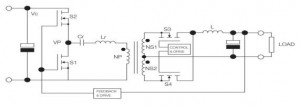
The topology of the main converter is resonant ZVS LLC (zero voltage switched inductor-inductor-capacitor, see diagram), where Lr in the diagram is actually the leakage inductance of the transformer.

With resonant topologies, points out Bocock, the important reactances tend to be the parasitics that do not make it onto conventional circuit diagrams.

ZVS LLC is variable frequency, increasing filtering complexity, but over a narrow range, which eases the situation.

LLC half-bridge is a popular topology around this power level, but knowing that is just the first step in making a good power supply.  “The theory is one thing, implementation is another,” said Bocock.

Output rectification is synchronous with mosfets to save power compared over the diode alternative. The active half-bridge secondary uses two winding and two mosfets. “I have not seen anyone use a full bridge secondary,” said Bocock.

One reason for this is the awkward gate drive needed for a four mosfet bridge.

Output mosfets are cooled by the considerable heatsink visible in the photo, which has grown since XP’s previous 2x4inch PSUs. These used similar rectification technology, but only had to deliver 120W with convection cooling or 180W forced.

Quasi-resonant power factor correction

The main power stage is preceded by a transition-mode quasi-resonant power factor correction (PFC) stage. This mode is discontinuous – current reaches zero – with the switch turning on at the bottom of the decaying voltage sinusoid – so not zero voltage switching but minimum voltage switching.

Topologies and design are chosen to minimises electrical noise because of its indirect effect on both physical size and power efficiency.

“If you want a very efficient power supply, you need to start from low noise because all those filters and snubbers waste energy,” said Bocock. Attention to noise generation allows filtering circuits in ELP225 to be fairly simple, he said.

Conducted and radiated noise meet the standards EN55011 and EN55022 for Class B conducted and Class A radiated EMI specifications.

According to Bocock, XP typically aims for an EMI noise margin of 6dB under standard test conditions to allow customers some leeway.

Somewhere else the customer needs a little flexibility is cooling as not everyone has access to thermal modelling or a heat expert. “Some just get the largest fan they can fit,” said Bocock.

An initial estimate of ambient temperature could be way out, or most of the air from a fan could go somewhere else.

Down-to-earth thermal design

To bring these issues down to earth, XP identifies critical points on the PSU to be measured once it is in the prototype. “The whole airflow thing is very difficult to predict. In the data sheet, we say measure the temperature of some specific components and make sure they do not get above temperature. If the temperature is lower than specified, it will meet all safety requirements,” said Bocock. “We recommend the customer always measures the temperatures of the electrolytics, just in case ambient is actually high, and we always try to put electrolytic life curves in the data sheet.”

For reference, for convection cooling XP measures its open frame flat, with the PCB at the bottom. This is probably the harshest orientation except for upside down, said Bocock. If they are mounted vertically or sideways, they are likely to run cooler. For forced air testing, PSUs are installed in a duct of around 40x75mm cross section.

The series comprises seven standard models with outputs from 12 to 48V. All also have a second (12V 500mA) output to drive a fan.

Supplied from 230V, average efficiency is 93% across the range (average of efficiencies with loads of 25, 50, 75 and 100% of 225W).

With no-load power consumption is less than 500mW.

Intended for industrial, IT and medical applications, the series complies with EN 60950-1 for IT equipment plus medical approvals ANSI/AAME/ 60601-1 and IEC/EN60601-1 3rd edition.

Temperature range is -20 to 70°C, derated above 50°C, warranty is three years, and the approved altitude limit is 5,000m.

Stockists include: Farnell element14, Digi-Key and XP Power.


steve bush

Simple BD768xFJ chip eases SiC into the mainstream

Rohm BD768x SiC controller

Rohm BD768x SiC controller

Rohm has introduced a silicon ac-dc controller chip for silicon carbide mosfets.

Rather than some multi-kW industrial motor drive, it is a simple 8pin ac-dc controller for 50W single-output designs.

“Until now there has not been a control IC that can sufficiently draw out the performance of SiC mosfets, particularly in ac-dc converter systems. As a result designers are faced with numerous problems related to power consumption and stability in a variety of high power applications,” claimed Rohm.

Called BD768xFJ, the firm is claiming a 6% efficiency gain over all-silicon designs, and no heatsink requirement in “50W-class power supplies”.

Included are protection functions that support operation at up to 690Vac, so it is suitable for general 400Vac industrial applications.

It is a quasi-resonant controller operating at up to 120kHz.

steve bush