 NASA has revealed a technique which dramatically cuts the power consumption of Wi-Fi comms, at least at the remote terminal.
Key is modifying the Wi-Fi base station to allow the transmitter of the remote terminal to be replaced by a modulated passive reflector.
“In a Wi-Fi radio, 70-80% of power is consumed generating Wi-Fi signal. If you only reflect, you save the transmit power,” Adrian Tang of NASA’s Jet Propulsion Laboratory told Electronics Weekly. Tang is working with Frank Chang at UCLA.
What returns to the basestation is not some pale shadow of Wi-Fi.
“You get PHY, header, and everything; you get real Wi-Fi comms back,” said Tang.
The scheme works like this:
The basestation is modified to emit a 20dBm continuous-wave (CW) sinewave at the Wi-Fi fundamental frequency, while the remote terminal has an antenna connected to a variable phase shifter and a load.
Even without the phase shifter, the remote terminal can amplitude-modulate reflected signals by switching the load between matched and short-circuit.
With the right phase shift options, the signal reflected back from the antenna can be a clean Wi-FI signal with modulation up to 16-QAM – and phase shifters can be as simple as switches connecting the antenna to transmission lines of various lengths.
Tang and Chang have implemented such a modulator, offering QPSK and ASK as well as covering 2.4 or 5.83GHz, on a CMOS chip – its 200µm2 footprint is small enough to be added to a baseband SoC.
“At the remote terminal, there is no synthesiser, no power amplifier, just a modulator; and the modulator is just a bunch of switches,” said Tang.
For the demonstrator, the chip also includes a pseudo-random number generator.
The basestation has a conventional Wi-Fi receiver chip, but it needs some help as its receive antenna gets the smaller-than-usual modulated signal, swamped by reflections of the original CW transmission from the local environment. The CW reflections add-up to a single CW signal of arbitrary phase and amplitude, and put reception well outside the dynamic range of conventional Wi-Fi chip front-ends.
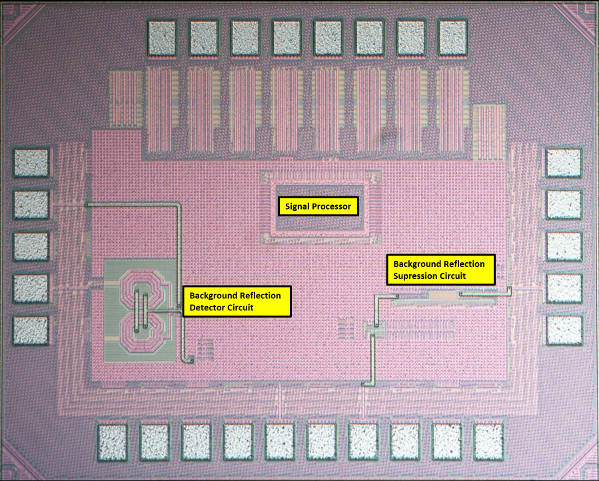
To get over this, Tang and Chang have created a second chip (see photo) which sits between the basestation receive antenna and the conventional Wi-Fi chip.
The second chip, made in 65nm CMOS, takes a sample of the transmitted CW signal and, via a variable phase shifter and a variable attenuator (right in the photo), adds it to the received signal.
With the correct phase shift and attenuation, most of the incoming CW signal can be nulled, leaving the Wi-Fi signal. Feedback loops in the on-chip signal processor updates phase and amplitude settings every 100µs.
“We can get about 60dB of suppression. We don’t actually need it all. We only need to stop the receiver from compressing,” said Tang. “10-20dB is good enough for a normal Wi-Fi chip.”
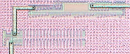
 In the photos, the central block is the signal processor. The right-hand circuit samples the CW transmit signal. Its two horizontal structures are a variable phase shifter above a variable attenuator.
On the left hand side is the antenna interface circuit.
So far, the scheme has been tested at up to 6m, with 330Mbit/s achieved at 2.5m range.
One fly-in-the-ointment is that Wi-Fi basestations are not permitted to transmit CW signals.
“We are working to make it 100% Wi-Fi standard compatible,” said Tang.
Patents have been applied for and applications in wearables where battery life is important are expected , said NASA, adding: “There are agreements in place for the commercialisation of the technology.”
The idea behind the scheme came out of a NASA project to eliminate mechanically-steered antennas in space – whose pivots have a habit of seizing, according to Tang.
Conventionally, the mechanically-fixed alternative is beam-forming using a fixed planar array of antennas, each driven by a separately phase-shifted signal through its own power amplifier, or low-noise amplifier (LNA) in the receive case.
NASA instead is experimenting with a single power amplifier and fixed antenna, bouncing its energy off a fixed planar array of reflective antennas, each with its own variable phase-shifter to steer the beam. If it works, it will remove the need for multiple power amplifiers or LNAs.