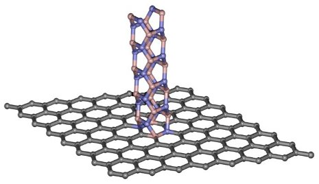
Two dimensional tin has been fabricated by a Chinese-American team. It is potentially a large band-gap semiconductor with unusual properties that include topological superconductivity and near-room-temperature quantum anomalous Hall effect, according to the Nature Materials paper ‘Epitaxial growth of two-dimensional stanene‘.
Topological superconductivity is the free conduction of electrons along the outside edges of a two dimensional material.
Stanene now joins 2D silicon (silicene) and 2D germanium (germanene) from group IV of the periodic table.
The team found a suitable hexagonal crystal to grow it on – (111) Be2Te3 – and deposited it using molecular beam epitaxy – MBE was how other teams managed to fabricates silicene and germanene, and germanene has also been made by mechanical exfoliation.
What grows is not totally flat like graphene, but a molecule with a regular slight buckle – every second atom is either slightly up or slightly down from the molecular plane – resembling two layers when viewed from the side. The height difference is around 0.1nm.
This is early days for the material, which interacted with the substrate and could not be measured in isolation. Work with the bare substrate, the substrate plus stanene, and then further over-coated with potassium, allowed theoretical models to be confirmed and improved. “The synthesis of stanene and its derivatives will stimulate further experimental investigation of their theoretically predicted properties”, said researchers in the paper’s abstract.
Scientists took part from: Shanghai Jiao Tong University, Stanford University, Tsinghua University, Collaborative Innovation Center of Quantum Matter (Beijing) and Collaborative Innovation Center of Advanced Microstructures (Nanjing).