Author Archives: steve bush

Plessey retrofitting with its own lighting LEDs

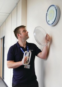
Plessey is retrofitting its Plymouth manufacturing facility with LEDs and lighting modules made on-site.

Plessey is retrofitting its Plymouth manufacturing facility with LEDs and lighting modules made on-site.

Plessey is retrofitting its Plymouth manufacturing facility with LEDs and lighting modules made on-site.

It will replace fluorescent tubes and compact fluorescent bulbs in existing fixtures – approximately 2,700 fixtures replacing 4,200 fluorescent lamps – for which it has designed retrofit kits.

“LED retrofit kits offer the facilities engineers and installation contractors a cost effective, quick and easy method to take advantage of the new technology, said Plessey facilities engineer Thomas Abbott. “It only takes five to 10 minutes to retrofit a fixture.”

There are three main types of fixture: batten, pod-style down-light and reflector ceiling troffer, plus high bay and low bay HID fixtures.

Current site lighting power consumption per year is 1,000,000kW/h costing £100,000, said the firm, plus approximately £5,000 in materials and 200 man hours annually.

“Once the retrofit is completed, the company would expect to see 25% – 40% reduction in lighting electricity consumption, saving tens of thousands of pounds per year,” said Plessey.

See alsoPlessey selling GaN-on-Si LED die

See alsoPlessey goes into LED light bulb ‘filament’ production

View more Plessey stories on Electronics Weekly »


steve bush

Electricity meter sticks on circuit breakers

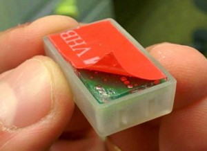
Berkely Labs stick-on electricity meterBerkeley Lab researchers have developed a peel-and-stick electricity meter which allows individual circuits in the home and industry to be accurately monitored.

It is an alternative to current transformers and live voltage connections that can be installed without mains voltage working expertise as the sensors are simply stuck to the front of each circuit breaker in a consumer unit. The only critical steps are aligning the sensor before sticking, and identifying the breaker type to the system so that calibration parameters can be loaded.

Each sensor is 19 x 12mm including a capacitive voltage pick-up and a Hall-effect current probe. They are daisy-chained with ribbon cable which supplies power (5V 16mA) and takes serial data back to a local wireless node – based on a Raspberry Pi in the experiment. This links with a remote laptop running system monitoring algorithms, written in Python.

Most circuit breakers have similar internal structures, which makes the technique broadly applicable. There are two types in the US, according to the Lab: bimetallic thermal and solenoid magnetic. The thermal type was chosen for testing because its lower magnetic field (10-20x) made it the toughest challenge for current sensing.

Inside, the voltage probe is the bottom layer of the internal PCB and the Hall sensor is an Allegro A1301. Both signals are conditioned by op-amp-based filters and fed into the 10bit ADC of a MSP430G2131 microcontroller for serialisation and transmission along the ribbon cable.

1,920sample/s are sent – a multiple of the 60Hz line frequency to simplify subsequent fast Fourier transforms, and fast enough for mains harmonics to be captured.

Time averaging is included to increase the signal-to-noise ratio of the Hall effect probe, and the laptop runs fairly complex power estimation algorithms that include software phase locked loops to track input waveforms. Calibration is required once per breaker type.

There is considerable cross-talk from adjacent circuit breakers, and an adaptive algorithm reduces errors from this to 5% after 15min of operation without any need for calibration via known loads.

Voltage measurements are within 1% of conventional contact probing, power below 10W can be resolved, and complex loads like triac dimmers can be handled.

More information on the algorithms is available in ‘COTS-Based Stick-On Electricity Meters for Building Submetering‘, published in the IEEE Sensors Journal.

steve bush

Molecular diode with 200:1 conduction ratio

Berkeley diode Jeff Neaton

Columbia University and Berkeley Labs have created a molecular diode with a forward/reverse current ratio in excess of 200 at fixed voltage

Columbia University and Berkeley Labs have created a molecular diode with a forward/reverse current ratio in excess of 200 at fixed voltage.

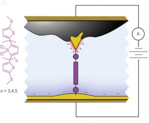
The molecule, designed at Columbia, is an oxidised thiophene derivative, with molecular resonance in nearly perfect alignment with the Fermi electron energy levels of the gold electrodes, according to Berkeley Labs.

It is a symmetrical molecule in an ionic solution, with asymmetry coming from different sized gold electrodes – see diagram.

“Electron flow at molecular length-scales is dominated by quantum tunnelling,” said Jeff Neaton, director of Berkeley Labs’ Molecular Foundry. “The ionic solution, combined with the asymmetry in electrode areas, allows us to control the junction’s electrostatic environment simply by changing the bias polarity. In addition to breaking symmetry, double layers formed by ionic solution also generate dipole differences at the two electrodes, which is the underlying reason behind the asymmetric shift of molecular resonance.”

Work at Columbia confirmed no rectification happened in non-ionic solution.

“We expect the understanding gained from this work to be applicable to ionic liquid gating in other contexts, and mechanisms to be generalised to devices fabricated from two-dimensional materials,” said Brian Capozzi of Columbia, adding that the molecular circuit is also revealing new routes to charge and energy flow at the nanoscale.

The work is convered by a Nature Nanotechnology paper: ‘Single-molecule diodes with high rectification ratios through environmental control’.

Image: Jeff Neaton, director of Berkeley Labs

steve bush

Molecular diode with 200:1 conduction ratio

Berkeley diode Jeff NeatonColumbia University and Berkeley Labs have created a molecular diode with a forward/reverse current ratio in excess of 200 at fixed voltage.

The molecule, designed at Columbia, is an oxidised thiophene derivative, with molecular resonance in nearly perfect alignment with the Fermi electron energy levels of the gold electrodes, according to Berkeley Labs.

It is a symmetrical molecule in an ionic solution, with asymmetry coming from different sized gold electrodes – see diagram.

“Electron flow at molecular length-scales is dominated by quantum tunnelling,” said Jeff Neaton, director of Berkeley Labs’ Molecular Foundry. “The ionic solution, combined with the asymmetry in electrode areas, allows us to control the junction’s electrostatic environment simply by changing the bias polarity. In addition to breaking symmetry, double layers formed by ionic solution also generate dipole differences at the two electrodes, which is the underlying reason behind the asymmetric shift of molecular resonance.”

Work at Columbia confirmed no rectification happened in non-ionic solution.

“We expect the understanding gained from this work to be applicable to ionic liquid gating in other contexts, and mechanisms to be generalised to devices fabricated from two-dimensional materials,” said Brian Capozzi of Columbia, adding that the molecular circuit is also revealing new routes to charge and energy flow at the nanoscale.

The work is convered by a Nature Nanotechnology paper: ‘Single-molecule diodes with high rectification ratios through environmental control’.

steve bush

Low phase noise for VCXO

Crystek is claiming record low phase noise for its voltage-controlled crystal oscillator (VCXO) - CVPD-922

Crystek is claiming record low phase noise for its voltage-controlled crystal oscillator (VCXO) – CVPD-922

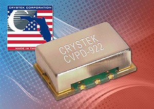
Crystek is claiming record low phase noise for its voltage-controlled crystal oscillator (VCXO): -85 dBc/Hz at 10Hz offset.

Called CVPD-922, typical phase jitter is 85fs (12 kHz to 20 MHz) and noise floor is -162 dBc/Hz.

Frequency options are between 40 and 125MHz.

Size is 14.2 x 9.14 x 5.3mm high

HD video broadcast equipment is one potential application.

Phase noise
10Hz -85dBc/Hz Typical
100Hz -115dBc/Hz Typical
1kHz -145dBc/Hz Typical
10kHz -155dBc/Hz Typical
100kHz -160dBc/Hz Typical
1MHz -162dBc/Hz Typical
10MHz -162dBc/Hz Typical

steve bush

Manufacturing jobs climb – Recruitive

recruitiveJuly saw a significant increase in the number job vacancies advertised within the manufacturing industry, according to recruitment software provider Recruitive.

The number of manufacturing jobs advertised via Recruitive’s multi-posting software increased by a 23% in July compared to June, which follows a steady month on month increase for over 2 years. The average number of candidate’s applying for each position has also seen an increase in July.

“Despite the index rising more than forecast in July to 51.9, it remains well below an average of 54.3 recorded in April 2013, when Britain’s economy was starting its recovery,” said Recruitive MD Richard Clarke.

“Our figures support the statistics from the latest Markit/CIPS Purchasing Manager Index [PMI], which suggest that UK manufacturing growth picked up in July from a 26 month low in June, and also that employment within the sector rose for the twenty-seventh successive month.”


steve bush

Ergonomics of Bloodhound

Cambridge Design Partnership Bloodhound

Cambridge Design Partnership Bloodhound

Cambridge Design Partnership has re-worked the design of Bloodhound’s steering wheel.

“The initial steering wheel design was created by the Bloodhound team using a number of novel design techniques including bio-mimicry, crowd sourcing and drawing on experience from Thrust SSC,” said the Parnership.

According to the firm, the original geometry of the grip area was retained from a clay model supplied, while push buttons were relocated.

“The new layout now allows a single fluid rotation movement of the thumb to transition from the power grip used when driving into an activation grip required to press buttons. This revised position could save between 0.5 and 3 football pitches of distance during the deceleration phase of each run,” said the Partnership, adding that it also “incorporated swooping curves across the top and bottom of the steering wheel to add a dynamic aesthetic” and give a clear view of the instruments.

The steering wheel was fabricated in titanium using additive manufacturing.

steve bush

Toshiba stacks 16 NAND die using TSVs

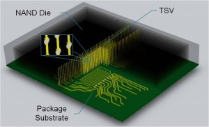
Toshiba x16 stacked nand flashToshiba has used through silicon vias (TSVs) to connect up to 16 stacked die in a range NAND flash chips.

The prototype will be shown at Flash Memory Summit in Santa Clara next week.

“Prior art stacked NAND flash memories are connected together with wire bonding in a package,” said the firm.

“TSV technology instead utilises the vertical electrodes and vias to pass through the silicon dies for the connection. This enables high-speed data input and output, and reduces power consumption.”

I/O data rate is >1Gbit/s with 1.8V to the core and 1.2V I/O.

High-end enterprise solid-state drives are a potential application.

New Energy and Industrial Technology Development Organization (NEDO) developed some of the technology.

toshstackPrototype specification:

package NAND dual x8 BGA-152 NAND dual x8 BGA-152
Gbyte 128 256
die stacked 8 16
width mm 14 14
depth 18 18
height 1.35 1.90
interface toggle DDR toggle DDR

steve bush

Stanene: two-dimensional tin

Two-dimensional tin, Stanene, has been fabricated by a Chinese-American team. It is potentially a large band-gap semiconductor with unusual properties that include topological superconductivity and near-room-temperature quantum anomalous Hall effect, according to the Nature Materials paper ‘Epitaxial growth of two-dimensional stanene‘.

Topological superconductivity is the free conduction of electrons along the outside edges of a two dimensional material.

Stanene now joins 2D silicon (silicene) and 2D germanium (germanene) from group IV of the periodic table.

The team found a suitable hexagonal crystal to grow it on – (111) Be2Te3 – and deposited it using molecular beam epitaxy – MBE was how other teams managed to fabricates silicene and germanene, and germanene has also been made by mechanical exfoliation.

What grows is not totally flat like graphene, but a molecule with a regular slight buckle – every second atom is either slightly up or slightly down from the molecular plane – resembling two layers when viewed from the side. The height difference is around 0.1nm.

This is early days for the material, which interacted with the substrate and could not be measured in isolation. Work with the bare substrate, the substrate plus stanene, and then further over-coated with potassium, allowed theoretical models to be confirmed and improved. “The synthesis of stanene and its derivatives will stimulate further experimental investigation of their theoretically predicted properties”, said researchers in the paper’s abstract.

Scientists took part from: Shanghai Jiao Tong University, Stanford University, Tsinghua University, Collaborative Innovation Center of Quantum Matter (Beijing) and Collaborative Innovation Center of Advanced Microstructures (Nanjing).


steve bush