Cypress has introduced what it claims is the lowest power energy harvesting power management IC (PMIC), usable with solar cells down to 10x10mm.
 Aimed at wireless sensor nodes, and called S6AE101A, it will start when 1.2uW is available and continue to function on as little as 250nA. According to the firm, 1.2μW is available at 65 lux from a 10 x 10mm solar cell.
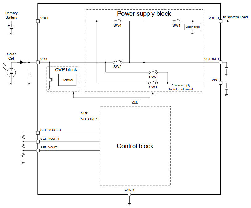
The linear chip mediates between a solar cell, an optional non-rechargeable battery, a load and two storage capacitors (one for the load and one for internal circuits), and is built into the firm’s EZ-BLE PRoC wireless sensor node module, which also includes a Bluetooth LE radio.
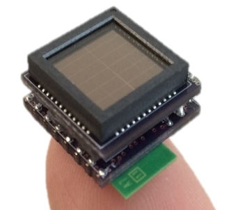
The module (pictured) squeezes a lot under a 10 x 10mm PV cell: ARM Cortex-M0, Bluetooth radio, two crystals, chip antenna, metal shield and passive components.
“The most compelling wireless sensor nodes that will drive IoT growth are self-powered, can be deployed anywhere for more than 10 years, and require minimal deployment and maintenance costs,” said Kiyoe Nagaya, v-p of Cypress analogue business. “Our energy harvesting PMIC and smart module enable developers to create solar-powered wireless sensor nodes for battery-less IoT devices.”
S6AE101A came though the firm’s Spansion subsidiary, and is sampling now. It is the first of a family with at least two other chips: S6EA102A and S6EA103A, both of which add a second power gating switch for a second output at the expense of 30nA more quiescent current. Both also include a 400nA Iq linear regulator. The …103A also has two more timers and a 20nA comparator.
The second power gated output has its own storage capacitor, and a more sophisticated version of the …101A controller block implements various operating modes using the hardware resources.
Cypress offers a Solar-Powered IoT Device Kit that contains a baseboard with a solar module and a Bluetooth Low Energy-USB bridge.
PMIC software support comes through a web tool called Easy DesignSim.
 S6AE101A at a glance
- Min solar cell size 1cm2 ( ~100 lux min)
- Solar cell input 2.0-5.5 V
- Battery input 2.0-5.5 V
- Output voltage 1.1-5.2 V
- Quiescent 250 nA
- Start-up 1.2 μW
- Six power gating switches
- Over-voltage protection
- 3x3mm 10pin SON


