Author Archives: steve bush

Perovskite solar: Good, with a dark side

Perovskite IDTechExPerovoskite photovoltaics promise >20% efficiency, low cost materials and flexible, stretchable, transparent variants, but are destroyed by damp and emits poison as they die.

So says a report by Cambridge market research firm IDTechEx.

Organolead halide perovskites are the promising technology because they absorb light efficiently.

“Flexible stretchable versions have been produced by Johannes Kepler University in Austria. With 100% yield, exhibiting 12% efficiency, they are only 3μm thick and weigh 5.2g/m2,” said IDTechEx chairman Dr Peter Harrop. However, “PbI, one of the breakdown products of the perovskite, is both toxic and carcinogenic. A glass panel can be made hermetically sealed, but plastics can be easily pierced”. These reactive iodides also corrode the metal electrodes.

So glass versions are fine, providing they are recycled at end-of-life, and plastic versions are in need of a barrier layer to keep moisture out and Pb compounds in.

Pb-free perovskites have poor efficiency, but may find niches.

Progress is being made.

“New perovskite solar cells with 16% efficiency have been developed by researchers from Switzerland and China. Stable and moisture resistant, they overcome some of the problems of perovskites,” said IDTechEx.

Within these, an interlayer protects the metal, allowing the cells to preserve their efficiency for two days.

Stabilising cross-links in the material are formed by a phosphonic acid ammonium additive hooking together the perovskite crystallites through hydrogen bonding with the phosphorus and nitrogen-containing terminal groups of the linker molecule.

The additive apparently allows the perovskite to be incorporated uniformly in an on the surface of a mesoporous titanium dioxide scaffold material.

Efficiency rises from 8.8 to 16.7% and the cations passivate the surface against water molecules.

IDTechEx has published a report: ‘The rise of perovskite solar cells 2015-2025′.

The sublect will also be covered by Belgian research lab IMEC and IDTechEx at the IDTechEx Show in Santa Clara (18-19 November).

steve bush

Perovskite solar: Good, with a dark side

Perovskite IDTechExPerovoskite photovoltaics promise >20% efficiency, low cost materials and flexible, stretchable, transparent variants, but are destroyed by damp and emits poison as they die.

So says a report by Cambridge market research firm IDTechEx.

Organolead halide perovskites are the promising technology because they absorb light efficiently.

“Flexible stretchable versions have been produced by Johannes Kepler University in Austria. With 100% yield, exhibiting 12% efficiency, they are only 3μm thick and weigh 5.2g/m2,” said IDTechEx chairman Dr Peter Harrop. However, “PbI, one of the breakdown products of the perovskite, is both toxic and carcinogenic. A glass panel can be made hermetically sealed, but plastics can be easily pierced”. These reactive iodides also corrode the metal electrodes.

So glass versions are fine, providing they are recycled at end-of-life, and plastic versions are in need of a barrier layer to keep moisture out and Pb compounds in.

Pb-free perovskites have poor efficiency, but may find niches.

Progress is being made.

“New perovskite solar cells with 16% efficiency have been developed by researchers from Switzerland and China. Stable and moisture resistant, they overcome some of the problems of perovskites,” said IDTechEx.

Within these, an interlayer protects the metal, allowing the cells to preserve their efficiency for two days.

Stabilising cross-links in the material are formed by a phosphonic acid ammonium additive hooking together the perovskite crystallites through hydrogen bonding with the phosphorus and nitrogen-containing terminal groups of the linker molecule.

The additive apparently allows the perovskite to be incorporated uniformly in an on the surface of a mesoporous titanium dioxide scaffold material.

Efficiency rises from 8.8 to 16.7% and the cations passivate the surface against water molecules.

IDTechEx has published a report: ‘The rise of perovskite solar cells 2015-2025′.

The sublect will also be covered by Belgian research lab IMEC and IDTechEx at the IDTechEx Show in Santa Clara (18-19 November).
steve bush

30W mains chip improves cross-regulation without opto-couplers

Power Int Innoswitch EP schematic

Power Int Innoswitch EP schematic

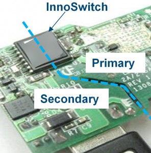
Power Integrations is aiming at domestic appliances the next iteration of its FluxLink in-package inductive feedback technique for secondary-side regulation without opto-couplers.

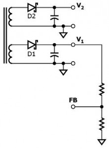
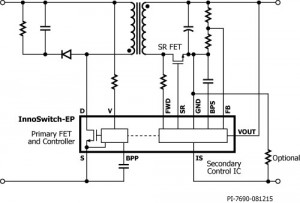
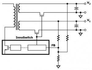
The chips, to be known as the InnoSwitch-EP family, have three die within a single package: a 725V primary-side switching mosfet, a primary-side control IC, and a secondary-side control IC – see diagram. The secondary-side synchronous rectifier mosfet is an external component.

Within the package, primary and secondary components are separated by a safety-rated dielectric barrier.

Feedback from secondary-side to primary-side IC across the barrier is through an inductive coupler constructed from bond-wires and the two lead-frames. Exactly the scheme works is not something the firm likes to talk about, except to say it gives good output regulation (+/-3% voltage, +/-5%), and that it is highly resistant magnetic interference from outside.

It also uses less static power than an opto-isolator – no-load power for a single output version can be under 10mW at 230 Vac when supplied by transformer bias winding.

Power Int Innoswitchdual outputMultiple output power supplies with good cross-regulation are possible without resorting to separate primary components.

This is due to synchronous rectification and sensing both outputs (compare output diagrams).

With diodes rectifiers and single output sensing, the un-sensed output not only has variation it its own diode’s voltage drop to contend with as its load varies, but its winding voltage will also vary as the current though diode on the regulated output varies from min to max, varing its Vdiode by 200-300mV.

With synchronous rectification, the mosfets drop only tens of mV, reducing interaction between the outputs, and the two-input potentiometer weights feedback to reduce it further.

Power Int non-Innoswitchdual outputReduced voltage drops through synchronous rectification also increase efficiency.

“For example, InnoSwitch-EP ICs enable 20W power supplies to achieve approximately 90% efficiency in a multi-output design, while minimising no-load consumption to less than 30mW,” said the firm. “They enable designers to meet new ENERGY STAR 7 efficiency standards for monitors.”

Particularly for countries where mains line voltage is poorly controlled, input voltage is sensed and switching paused if the input exceeds 320Vac. Switching re-commences when it drops to a safe level for over 150ms. According to Power Integrations, line over-voltage sensing is +/-5%.

Applications are expected in microwaves, washers and dryers, as well as in stand-by power supplies for PCs, servers, air conditioning, displays, TVs, and lighting.

Samples are available now, as is a reference design (RDK-469).

PowerInt Innoswitch app photoDevices at a glance – power is for open-frame design, or peak in an enclosure.

230Vac +/-15% 85-265Vac
INN2603K 24W 15W
INN2604K 27W 20W
INN2605K 35W 25W

steve bush

30W mains chip improves cross-regulation without opto-coupler

Power Int Innoswitch EP schematicPower Integrations is aiming at domestic appliances the next iteration of its FluxLink in-package inductive feedback technique for secondary-side regulation without opto-isolators.

The chips, to be known as the InnoSwitch-EP family, have three die within a single package: a 725V primary-side switching mosfet, a primary-side control IC, and a secondary-side control IC – see diagram. The secondary-side synchronous rectifier mosfet is an external component.

Within the package, primary and secondary components are separated by a safety-rated dielectric barrier.

Feedback from secondary-side to primary-side IC across the barrier is through an inductive coupler constructed from bond-wires and the two lead-frames. Exactly the scheme works is not something the firm likes to talk about, except to say it gives good output regulation (+/-3% voltage, +/-5%), and that it is highly resistant magnetic interference from outside.

It also uses less static power than an opto-isolator – no-load power for a single output version can be under 10mW at 230 Vac when supplied by transformer bias winding.

Power Int Innoswitchdual outputMultiple output power supplies with good cross-regulation are possible without resorting to separate primary components.

This is due to synchronous rectification and sensing both outputs (compare output diagrams).

With diodes rectifiers and single output sensing, the un-sensed output not only has variation it its own diode’s voltage drop to contend with as its load varies, but its winding voltage will also vary as the current though diode on the regulated output varies from min to max, varing its Vdiode by 200-300mV.

With synchronous rectification, the mosfets drop only tens of mV, reducing interaction between the outputs, and the two-input potentiometer weights feedback to reduce it further.

Power Int non-Innoswitchdual outputReduced voltage drops through synchronous rectification also increase efficiency.

“For example, InnoSwitch-EP ICs enable 20W power supplies to achieve approximately 90% efficiency in a multi-output design, while minimising no-load consumption to less than 30mW,” said the firm. “They enable designers to meet new ENERGY STAR 7 efficiency standards for monitors.”

Particularly for countries where mains line voltage is poorly controlled, input voltage is sensed and switching paused if the input exceeds 320Vac. Switching re-commences when it drops to a safe level for over 150ms. According to Power Integrations, line over-voltage sensing is +/-5%.

Applications are expected in microwaves, washers and dryers, as well as in stand-by power supplies for PCs, servers, air conditioning, displays, TVs, and lighting.

Samples are available now, as is a reference design (RDK-469).

PowerInt Innoswitch app photoDevices at a glance – power is for open-frame design, or peak in an enclosure.

230Vac +/-15% 85-265Vac
INN2603K 24W 15W
INN2604K 27W 20W
INN2605K 35W 25W

steve bush

Leti fabs MEMS on 300mm wafers

Leti fabs MEMS on 300mm wafers

Leti fabs MEMS on 300mm wafers

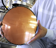
French research fab CEA-Leti has manufactured accelerometers on 300mm wafers, thought to be a first for the MEMS industry.

“This demonstration that our 200mm MEMS platform is now compatible with 300mm wafer fabrication shows a significant opportunity to cut MEMS production costs,” said Leti CEO Marie Semeria. “This will be especially important with the expansion of the Internet of things and growing demand for MEMS in mobile devices.”

This is Leti’s ‘M&NEMS’ technology, based on detection by piezo-resistive silicon nanowires, which is claimed to reduce the size of multi-axis sensors. It also allows fabrication of combination sensors – for example three-axis accelerometer plus three-axis gyroscope plus three-axis magnetometers on the same chip. It is currently being transferred to “an industrial partner”, said the lab.

In addition: “manufacturing MEMS with 300mm technology enables 3D integration using MEMS CMOS processes in more advanced nodes than on 200mm, and the use of 3D through-silicon-vias, which is already available in 300mm.”

Details are being presented at the European MEMS Summit this week.


steve bush

Rohm tackles USB Type-C power

Rohm USB Type-C power

Rohm USB Type-C power

ROHM has developed power receiver controller ICs compatible with USB Power Delivery (Rev2.0) and Type-C (Rev1.1).

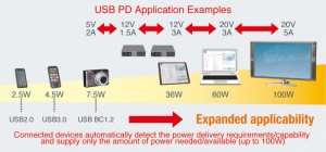
BM92TxxMWV series supports conventional USB power up to 7.5W, all the way up to 100W (20V 5A) for USB Type-C connected devices.

“This will make it possible to drive equipment with larger power requirements such as TVs and PCs via USB and at the same time enable conventional USB-equipped portable devices – smartphones and tablets – to be charged up to four times faster than the previous standard,” said Rohm.

“The latest USB connector and power transmission standards developed by USB-IF [USB Implementers Forum], which includes USB Type-C, USB Power Delivery, USB Superspeed and the new DisplayPort Alternate Mode standard for carrying video, are garnering increased attention as a true all-in-one cable solution by making it possible to deliver high power, high-speed data, and even 4K video simultaneously over a single USB cable/port. This will eliminate the need for dedicated cables, providing greater convenience while reducing clutter and waste.”

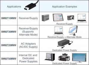
Rohm USB Type-C product lineThe firm has used a 0.13um BiCDMOS processes for its IC, eliminating the need for an external fet and it power supply.

For the Power Deliver standard, optimum power delivery is enabled in both directions along a USB Type-C connection through a power contract that determines the Provider (Supply) and Consumer (Receiver) devices.

The Consumer only requests the required amount of power and the Provider only supplies the power available.

Power delivery scales from 7.5W (5V 1.5A) up to 100W (20V5A) – see diagram.

DisplayPort Alternate Mode carries video signals over USB, eliminating the need for dedicated video cables.

Price is $16.5/unit, and the chip is sampling this month with OWM quantities expected in December.

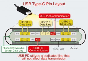
USB Type-C layout - from RohmUSB Type-C

Defined under USB3.1, USB Type-C is a receptacle (concave connector), plug (convex connector), and cable standard.

Cables are reversible and flippable – so the connector fits either way around and the ends can be swapped too.

Power requirements are negotiated between connected devices to determine the upstream and downstream facing ports (UFP and DFP), providing greater convenience and utility.

steve bush

Freescale replaces traditional car batteries with Li-ion

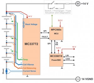
Freescale MC33772Freescale Semiconductor has announced a lithium-ion cell controller with performance and functional safety features optimised for 14V car batteries, intended to replace traditional Pb-acid automotive batteries.

“Lead-acid automotive batteries are increasingly being replaced by Li-ion chemistries to reduce weight, increase reliability and boost energy efficiency for engine start-stop systems and energy recuperation technologies,” said the firm. “Recent advances in Li-ion battery chemistry for cold temperature operation and cold cranking power now enable Li-ion batteries to displace lead-acid even as the starter battery.”

While Pb-acid batteries are heavy,  it is one of the battery technologies least likely to explode or bust into flames.

In contrast, many Li-ion chemistries are flammable, requiring close monitoring, and all of them need tight control of charge voltage to balance life with energy density.

“To maintain safe operating conditions and ensure system-wide control of the battery, battery cell controllers must provide accurate, reliable battery diagnostics and high speed communication of status,” said Freescale.

The chip, called MC33772, includes functional verification supporting ISO 26262 ASIL-C requirements, which help protect automotive batteries against critical fault conditions. ASIL-D (higher level) system implementations be realised using multiple Freescale battery cell controllers for redundancy. For functional safety design to ISO 26262 and IEC 61508, the chip is supported by Freescale’s SafeAssure programme.

It supports 2Mbit/s battery health and conditions communication for centralised, distributed CAN and distributed daisy chain battery management system topologies.

Freescale points out its battery controller portfoilio includes support for: lithium iron phosphate, lithium nickel manganese cobalt oxide, lithium titanate and lithium polymer cells, but it is not yet clear if the MC33772 can work with all of these.

MC33772 at a glance

  • AEC-Q100 automotive qualified
  • 3, 4, 5 and 6 cell versions
  • SPI direct-coupled communication
  • 2MHz isolated  TPL (transformer physical layer) communication using separate chip (MC33664)
  • 5-30V operation, 40V transient (7-30V with TPL comms)
  • Current sensor with ±0.5% accuracy from mA to kA
  • 6x differential cell voltage measurement and stack voltage measurement
  • Synchronised cell voltage/current measurement
  • Coulomb counting
  • 7x ADC/GPIO/temperature sensor inputs
  • Addressable on initialisation
  • 6x onboard 300mA passive cell balance drivers with timers
  • Low-power modes
  • 48pin QFP
  • Products are sampling now, with production planned by Q2 2016.

Evaluation kits KIT33772ASP1EVB and KIT33664EVB support the MC33772 and MC33664 transformer physical layer.

Conventional Li-ion cells cannot safely be charged at all at temperatures below 0C, and discharge power is severely limited – see this article at Cadex’s Battery University.

steve bush