Author Archives: steve bush

Updated: Fairchild puts current control into LLC PSUs

Fairchild FAN7688

Fairchild has launched an isolated dc-dc controller chip which adds current-mode control to LLC resonant power supplies.

Called FAN7688, it has ‘charge current control’, instead of the voltage mode control traditionally used for LLC. “This “allows for tighter and faster output regulation against load transients and also simplifies the control loop,” said Farichild.

Update: see below for more technical detail, courtesy of Fairchild.

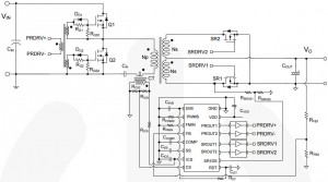
The technique involves combining a triangular waveform from the oscillator (see below) with the integrated switch current information to determine switching frequency, providing “a better control-to-output transfer function of the power stage simplifying the feedback loop design while allowing true input power limit capability”, said Fairchild.

Closed-loop soft-start prevents saturation of the error amplifier and allows monotonic rising of the output voltage regardless of load condition.

For improved efficiency, output rectification is synchronous using adaptive dead time control to reduce body diode conduction time – something branded ‘adaptive dual edge tracking secondary side synchronous rectifier control’.

Efficiency for a for 400V in and 12V out power supply is “typically up to 97%”, according to a Fairchild FAN7688 video – (interesting after a slow start)

Operating frequency spans 39-690kHz, and the chip works over -40 to +125°C.

Protection includes over-load, over-current, output-short and over-voltage.

Applications are expected in servers, telecoms, industrial, PCs and TVs.

There are two evaluation boards: 306W FEBFAN7668 and 250W FEBFAN7688A.

A little more detail
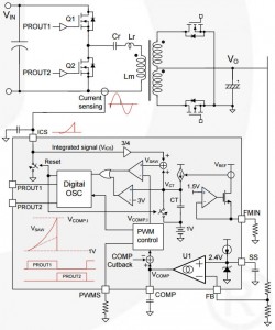
Fairchild FAN7688 controlPrimary-side switch current does not increase monotonically in resonant converter due to the sinusoidal current waveform, so it cannot be used for pulse frequency modulation (PFM) for output voltage regulation. Also the switch peak current, according to Fairchild, does not reflect load current because of large circulating currents included in the switch current.

However, the integral of primary side switch current (the primary charge) does increase monotonically and it’s peak value reflects the load current properly.

Primary side switch current is sensed through the current transformer (see diagram) – whose output is coupled to the FAN7688 and reset by the chip during half of the switching cycle to generate a proper charge signal. Then, this charge is compared with the control voltage to modulate the switching frequency.

Charge is proportional to average input current over a switching cycle, so it provides a fast inner loop with excellent transient performance including inherent line feed-forward.

CT, the PFM block timing capacitor is charged with a current set by the resistor on pin FMIN. Sawtooth waveform VSAW is the sum of the integrated primary current and and the timing capacitor voltage. This sum is compared with the compensation voltage to determine the switching frequency. Minimum switching frequency is set by a 3V limit in CT.

At light load, where circulating currents would be high, switching is shifted to PWM control.

Why use LLC, Fairchild explains:

The LLC resonant converter has been widely used becaus it can regulate the output over load variations with a relatively small variation of switching frequency.

It can achieve zero-voltage switching for the primary-side switches and zero-current switching for the secondary rectifiers over the entire operating range.

The resonant inductance can be integrated with the transformer into a single magnetic component.

Voltage-mode is typically used, where the error amplifier output voltage directly controls the switching frequency, However, compensation is relatively challenging since the frequency response with voltage control includes four poles and the locations of the poles changes with input voltage and load.

Charge current control is described in detail in the FAN7688 data sheet functional description section.


steve bush

Linux: Wind River moves to Yocto Project 2.0 kernel

Wind River has announced a new version of its Linux, promising a “significant reduction in set-up and installation time”, as well as a move to Yocto Project 2.0 kernel and tool chain.

yoctoIntended for Intel, ARM, MIPS, and PowerPC architectures, it is based on Linux kernel 4.1, and GNU toolchain 5.2, and is part of the firm’s Helix portfolio of products for IoT applications.

“Linux 8 will serve as the baseline for all existing technology profiles, including Carrier Grade Profile and Security Profile, for building and deploying a cloud operating system,” said the firm. “The new features enable cloud services and high-performance computing capabilities to integrate a compute node to a number of frameworks or infrastructure providers.”

The company also introduced new features for Wind River Open Virtualization.

Wind River is a member of the Yocto Project advisory board and a contributor, “contributing more than one third of the Yocto Project lines of code”, said Wind River.

The firm’s products can be seen at Embedded Linux Conference Europe this week in Dublin.


steve bush

Quantum cryptography demoes 200Gbit/s over 100km fibre

Toshiba quantum cryptography Toshiba’s Cambridge Research Lab has demonstrated 200Gbit/s quantum cryptography – quantum key protected data transmission – over a single 100km long cable, which is a world record.

It used six wavelength channels in total, two each at 100Gbit/s for the data and four including data and clock channels for the quantum keys.

One of the things that makes the scheme difficult is cross-talk: the conventionally encoded data bits are each represented by over a million photons, while bits in the quantum key are received on a single photon. Raman scattering spills data photons into the key channel.

“Lots of scattered light makes detecting key photons difficult,” Dr Andrew Shields, assistant MD of Toshiba Research Europe, told Electronics Weekly. “We filter the arriving key channel light in wavelength and time.”

Wavelength filtering is through a optical bandpass filter – narrower than those used in normal WDM (wavelength division multiplexed) fibre networks, and time filtering is based opening the receiver only when a key photon might be expected – a key photon is sent every nanosecond, signalled by the clock channel, and is around ~100ps long at the receiver.

Single photons

The key is encoded onto the phase of single photons. “We could encode polarisation, but we chose to use phase,” said Shields.

Detecting the phase of single photons at high speed is tricky to say the least.

For this 1Gphoton/s receivers has been developed that uses semiconductor-based avalanche photodiodes on each of two output ports of an interferometer – one for each expected phase state.

In quantum cryptography, the key is sent in a snoop-proof manner – according to the known laws of physics.

To send the key, pulses of photons are modulated with a key bit. Then, before they are launched into the fibre, they are heavily attenuated to have less than one photon per pulse on average – so some pulses have been completely absorbed.

Once in the fibre, remaining photons, which are still phase-modulated, either make it to the far end or is scattered away en-route.

Sender and receiver exchange information about which photons actually arrived, but not about the their states – ‘the first photon, the tenth photon, the……’, for example.

In this way, both ends know which photons arrived, and what their phase encoding was, but a snooper can only watch the back-channel and learn which photons arrived, not their phase.

Schrödinger’s cat

If the snooper tries to measure the phase as the photons pass, the phase will be corrupted – It is a Schrödinger’s cat situation, said Shields: “A man in the middle will change the encoding. There is nothing they can do to gain knowledge without changing the state of the encoded photons. They will always reveal themselves.”

Being able to send whole keys in less than 1ms means the key can be changed at more than 1kHz, cutting the length of data stream encoded with a single key, therefore further reducing the chance that statistical analysis will reverse-engineer the key from the encrypted data. For a fibre length of 36km, the secure key rate exceeds 1.9Mbit/s, sufficient for over 5,000 encryption keys per second.

For the record-breaking trial, which broke the Lab’s own 40Gbit/s record, Toshiba’s Cambridge Research Lab worked with ADVA Optical Networking (which provided the data transmission system) and BT’s R&D hub at Adastral Park near Ipswich where the demonstration took place.

Secure the genome

Toshiba is also involved in a system to secure genome data using quantum cryptography in Sendai, Japan.

This kind of data is unique in that it might have to stay secure for many human generations. “If it is encrypted using today’s technology, someone might save it [snooped data] and decrypt it when computers are more powerful,” said Shields. “You can’t do this with quantum encrypted data, even with quantum computers.”

Governments and banks are other potential users.

The next step in Cambridge is to build a network and demonstrate end-to-end quantum cryptography through that. According to Shields, his team has already demonstrated it working through an optical switch. “If the network is all-optical, we are able to form quantum keys end-to-end,” he said. “If it has electrical switching, the intermediate nodes have to be placed in a physically-secure area, for example at a telco or company office. There are ways to the possibility of attack against intermediate nodes: using secret sharing schemes, for example.”

EPSRC quantum key distribution networkThe Cambridge team is also collaborating in an EPSRC-funded long-term trial involving building a Cambridge-London-Bristol quantum cryptography network with metro networks at the Cambridge and Bristol nodes. Potential users will be able to use it for application development.

steve bush

Osram doubles stage lighting power

Osram doubles stage lighting power - LE RTDUW S2WN

Osram doubles stage lighting power – LE RTDUW S2WN

Following the uprating of its headlamp LED last week, Osram has done the same with its stage lighting flagship.

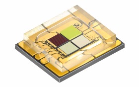
Thanks to improved chip technology, its latest multi-coloured four-chip Ostar Stage family can be operated at 2.5A – 30W total input power, double that of the previous version.

“The higher current which is necessary for a higher output requires the thermal management of the Osram Ostar Stage to be adapted so that the heat generated in the chip can be removed as effectively as possible”, said Osram product marketing manager Wolfgang Schnabel.

The 1mm² die are red, green, blue and white.

With the beam characteristics and package size as before, existing user can retain their existing optics and the overall design.

Other intended applications are mood and architectural lighting.

High volume production is scheduled for Q1 next year.

Ostar Stage LE RTDUW S2WN at a glance

Dimensions 4.68 x 5.75 x 1.26mm
Chip size 1mm²
Thermal resistance Rth 0.9K/W
Output 30W
Beam angle 120°

See alsoOsram reveals best headlamp LED yet

See more Osram stories on Electronics Weekly »

steve bush

UK firm harvest ambient RF for IoT

Drayson FreevoltAmbient RF signals are a viable source of energy, claims UK-based Drayson Technologies, which has patented a technique to harvest them.

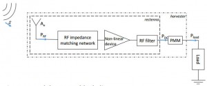
Branded Freevolt, it uses an antenna, ‘non-linear device’, RF filter and a power manager (PMM in diagram).

“To integrate Freevolt into different devices, Drayson Technologies has developed standard harvesters but can also provide different antenna and rectifier designs, depending on the application requirements,” said the firm, adding: it is important to note that a harvesting antenna can have different and unique characteristics depending on the application.

It gives the example of a device placed on a wall, where the antenna can be optimised to cover a broad angle and have the appropriate polarisation and frequency bands to take advantage of the maximum number of existing RF sources.

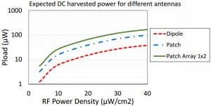
Drayson efficacyIn a white paper, the firm predicts efficacy, and describes ambient field measurement results that yielded 600-700nW/cm2 peak in a office block from Wi-Fi, GSM and 4G LTE, and a peak of 6.7uW/cm2 from 3G signals in busy outdoor London locations.

Drayson is marketing a UK-made RF-powered air quality sensor tag called CleanSpace. “This technology creates a crowd-sourced network of personal air sensors, initially across the UK and then expanding to major cities across the world, which will all be powered by Freevolt,” said the firm.

steve bush

AMD unveils PRO A-Series desktop and mobile processors

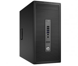
HP EliteDesk 705, with AMD PRO A-Series desktop processor

HP EliteDesk 705, with AMD PRO A-Series desktop processor

AMD has introduced its most powerful line of AMD PRO A-Series mobile and desktop processors.

Formerly called Carrizo and Godavari PRO, the processors are intended to run Windows 10, said AMD.

PRO A-Series Mobile 

These have the firm’s fastest mobile processor – version A12 running at up to 3.4GHz. There are 12 cores (4 CPU + 8 GPU).

Graphics are Radeon R7, with up to 800MHz clocking and 512 graphics compute cores. “It is the first commercial processor in the industry designed to be compliant with the Heterogeneous Systems Architecture [HSA] 1.0,” said AMD.

The device is ARM TrustZone hypervisor capable, enabling TrustZone to run on the on-board secure processor, and it has a HEVC (High-Efficiency Video Compression) decoder for streaming HD content.

The chips are already available in some HP EliteBook laptops.

PRO A-Series Desktop

“With support for Quick Stream PRO, the new AMD PRO desktop processors virtually eliminate the lag in latency-sensitive applications like VoIP and streaming video.,” said AMD, “Quick Stream PRO uses built-in intelligence to identify and allot more bandwidth for businesses’ highest priority applications.”

The chips are already installed some Lenovo M79 Towers and HP EliteDesk 705 Micro Towers.


steve bush

Wristband heart rate sensor includes DSP

AMS AS7000 in action - a wristband heart rate sensor

AMS AS7000 in action – a wristband heart rate sensor

AMS has launched an optical heart rate sensor for wrist wearables.

Called AS7000, it measures heart rate by shining light into blood vessels, which expand and contract as blood pulses through them, and analysing scattered reflections – which is called photoplethysmography (PPG).

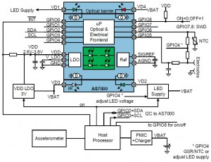
In a 6.1 x 4.1 x 1mm package, the device include two green LEDs and a photo-sensing signal processing IC – based around an ARM Cortex-M0. Green is chosen to best-sense pulse, and transducer spacing makes it most sensitive to scattering from an appropriate depth.

Although barriers in the package block light travelling direct from LEDs to photodiodes, said AMS, reflected pulse information is only a ~1% ripple on top of dc returns and large perturbations from movement.

“Unlike existing optical analogue front-ends which produce raw PPG readings, AS7000 integrates a digital processor which converts PPG readings into digital heart rate and heart rate variation”, claimed the firm.

AMS AS7000 photoTo work properly. the module has to be paired with an external accelerometer. This allows internal algorithms to filter-out the motion artefacts. “This means that the module can maintain high accuracy whether the user is resting or exercising.” said AMS.

The module also enables skin temperature and skin resistivity measurements through interfaces to and external thermistor and two skin electrodes.

Alongside the module, AMS is offering opto-mechanical design-in support which provides OEMs with electrical, mechanical and optical design guidelines to simplify optical design considerations such as air gap and glass thickness, and the design and material of the wrist strap and housing.

A wristband demonstration kit is available, which uploads readings via a Bluetooth interface board to an Android phone or tablet. An app presents results and allows real-time logging.

AMS has compared the demo kit to a traditional chest band sports heartrate sensor (Plolar RC3GPS) and claims close agreement.

AMS AS7000 app circuit

Application. Only green LEDs implemented in AS7000AA

AS7000AA AS7020 AS7024
MCU ARM Cortex M0 no no
memory 32k rom
4k ram
128byte FIFO 128byte FIFO
Analogue front ends 2 2 2
skin temp + resistance yes yes yes
ECG amplifiers no yes yes
LEDs green + green red + infra-red green + IR, green
Dimensions
mm (target)
6.1 x 4.1 x 1
20pin
0.4mm pitch
5 x 2.7 x 1
18pin
0.4mm pitch
6.1 x 2.7 x 1
20pin
0.4mm pitch
samples available available Nov. 2015
c-samples available Jan 2016 Feb/Mar 2016
Focus application Simple wristband phone Smart band / watch


steve bush

More on: Making MEMS on 300mm wafers

Leti MnNEMS accelermeter photo

Making MEMS on 300mm wafers

French research fab CEA-Leti has begun manufacturing accelerometers on 300mm wafers, thought to be a first for the MEMS industry.

“This demonstration that our 200mm MEMS platform is now compatible with 300mm wafer fabrication shows a significant opportunity to cut MEMS production costs,” said Leti CEO Marie Semeria. “This will be especially important with the expansion of the Internet of things and growing demand for MEMS in mobile devices.”

Leti has a 30 year history in making MEMS, spinning out MEMS companies, and selling MEMS processes to chip firms. It currently has a team of 200 people working on MEMS.

The transferred process is its ‘M&NEMS’ technology – micro and nano MEMS, which came out of a programme to make many types of micro-mechanical structures using a single straightforward process.

What emerged a way to make any mixture of the following sensors on the same chip: accelerometers (x, y and z axis), gyroscopes (x, y and z axis), magnetometers (x, y and z axis), pressure transducers and microphones.

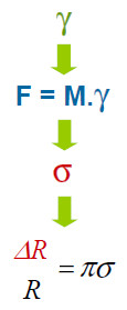
Capacitive (electrostatic) sensing has been avoided. Instead, for simplicity, all sensing is piezoresitive (piezo: Greek for squeeze).

“Piezoresistor sensing is robust, and importantly it is compact. We have miniature sensors, half the size of other peoples,” Jean-Rene Lequepeys, head of the Si component division at Leti, told Electronics Weekly.

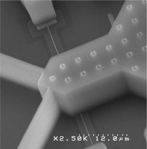
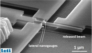
Not to be confused with piezoelectric sensing, detection is through measuring the change in resistance of silicon nano-wires (220x220nm2 cross-section) as the tension in them changes. This is the ‘NEMS’ part of the process name. In lithography terms, 220nm wire geometry means relaxed constraints on available lithography.

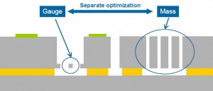
These wires are just visible close to the substrate in the photo, which is of the measurement end of a single axis accelerometer. The ‘proof mass’ whose movement is measured, and extends far to the right of the photo (see accelerometer diagram) is hewn from 20µm-thick epitaxial silicon – the ‘M’icro part of the process.

Leti MnNEMS accelermeter diagLeti MnNEMS accelermeter equationAs an aside, the two blade-like struts in the photo are the entire support structure for the proof mass – the rest of it is (see diagram below) cantilevered and free to move. Accelerometers for all three axis are constructed in the same plane

Construction starts with a Si-on-insulator wafer, prepared with a 220nm silicon top layer – which will yield the piezoresistors and the foundations of other structures. “We can develop the same technology on bulk silicon, but it is easier on SoI,” said Lequepeys.

Piezoresistors are patterned and etched from this 200nm layer, then protected by a temporary oxide covering.

Following this, 5-25µm of silicon is grown on top, from which masses and other MEMS structures are then etched – the buried oxide layer acting as an etch-stop.

NEMS and MEMS components are finally released by removing the oxide, including SoI wafer oxide, from around the piezoresistors and masses.

All the sensors mentioned earlier have been designed to be made from the same basic parts – a 220nm thick layer for piezoresitive gauges and the full later-grown thickness for masses and other parts.

Magnetometers, for example (which are sensitive enough to be used as compasses), are moving structures with a ferromagnetic layer deposited on top.

Leti MnNEMS cross section“For the magnetometer we use a balanced design to be not sensitive to the acceleration. It means that we have a symmetric design in order to have the centre of inertia that coincides with the rotation axis of the structure,” said Lequepeys.

The firm has transferred its technology Tronics Microsystems, which is making three accelerometers and three gyros within a <4mm2 footprint.

According to Lequepeys, while Leti can put triple accelerometers alongside triple gyros and triple magnetometers, competitors have to put the magnetometers on separate silicon. Type pressure monitors are a target for the process, as they need to combine an accelerometer and a pressure sensor.

300mm

According to Lequepeys, there are 97 process steps in M&NEMS, and a recipe for each has been adapted for 300mm production.

Moving the M&NEMS process to 300mm equipment is all about reducing the cost of MEMS production for consumer and automotive markets – at which M&NEMS is aimed. Ex-fab device costs are 30% cheaper in 300mm compared with 200mm, said Lequepeys.

300mm is also better for larger MEMS. “Auto-focus mechanisms are quite big devices, and so are digital loudspeakers and image-based sensors – for example for ultrasonic or micro-bolometer imaging,” he said.

Another reason for moving to 300mm is CMOS.

M&NEMS always uses a separate read-out chip to carry associated signal processing circuits. “We do MEMS and CMOS on the same wafer for other MEMS processes, but not M&NEMS,” said Lequepeys. “There are no major obstacles, but we would need to see an advantage in terms of cost.”

Both 200mm and 300mm processes at Leti offer 3d operations such as through-silicon vias (TSV), wafer thinning, wafer stacking and copper pillars which allow M&NEMS chips to be stacked with read-out chips, but while the 200mm process offers 130nm CMOS, 300mm opens the doors to 65, 45 and 28nm read-out processing.

Leti NEMS resonatorNEMS

Starting in a similar way, with an SoI wafer with thin top silicon, Leti has developed another process called ‘NEMS’.

Aimed at biological and chemical sensing, it runs only on Leti’s 200mm line. “The size of market not large enough to justify 300mm today,” said Lequepeys.

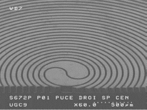
Sensing is once again though piezo-resistors, but there is no thick epitaxial layer. Instead, sensing structures are thin cantilevers made from the SoI wafer silicon (see photo right).

These cantilevers, which each have two piezoresistors, are vibrated by an oscillating electric field from a nearby electrode. The frequency at which they resonate is dependent on the mass of the cantilever and any mass on its surface.

NEMS has been used to develop a gas chromatograph in conjunction Caltech – the design of which is being exploited by a joint spin-out called Apix.

Leti NEMS chromatographA sample of gas fed into it passes through a long micro-machined channel (see photo right).

During the journey different molecules in the gas travel at different speeds, and by the time they reach the vibrating cantilever they can be sensed separately. Heating cleans out the sensor for repeated use.

Parts per million of many vapours can be can be detected, and sensitivity reaches parts per billion with heavy molecule like ethylbenzene.

Details of M&NEMS were presented at the European MEMS Summit earlier this month.

steve bush

Na-ion cathode is robust

eldfellite cathode for Na-ion cellSodium-ion (“Na-ion”) batteries could have taken another step to practicality as “safe and sustainable” cathode material is invented at the University of Texas at Austin.

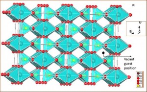
The material is the the non-toxic and inexpensive mineral eldfellite (NaFe(SO4)2).

“At the core of this discovery is a basic structure for the material that we hope will encourage researchers to come up with better materials for the further development of sodium-ion batteries,” said Preetam Singh, a postdoctoral fellow and researcher in Goodenough’s lab.

Sodium-ion batteries work just like lithium-ion batteries, but the materials are much cheaper. During the discharge, sodium ions travel from the anode to the cathode, while electrons pass to the cathode through an external circuit.

However, they have problems related to performance, weight and instability of materials.

The University’s cathode material addresses instability – its structure has fixed sodium and iron layers that allow sodium to be inserted and removed without damaging structural integrity.

Charge/gramme is two-thirds of that of a lithium-ion battery.

“We believe our cathode material provides a good baseline structure for the development of new materials that could eventually make the sodium-ion battery a commercial reality,” said Singh.

The wok is reported in the journal Energy & Environmental Science in a paper: ‘Eldfellite, NaFe(SO4)2: an intercalation cathode host for low-cost Na-ion batteries’.

UK start-up Faradion is attempting to exploit Na-ion cells.

steve bush