Author Archives: steve bush

Novel thulium fibre laser loop emits 2µm radiation

Novel thulium fibre laser loop emits 2µm radiation

2µm wavelength laser beams for medical and analytical use can be generated by a straightforward fibre laser, according to researchers at Ecole Polytechnique Fédérale de Lausanne Photonics Systems Laboratory (PHOSL) Techniques for generating 2µm light are nothing like as well developed as those for the telecoms wavelength of 1.55µm. According to PHOSL, to create a 2µ beam, ...

steve bush

Qualcomm reveals 24 core 64bit ARMv8-A server, and a deal with Xilinx

Qualcomm reveals 24 core 64bit ARMv8-A server, and a deal with Xilinx

Qualcomm has demonstrated pre-production versions of its finfet 24 core 64bit ARMv8-A processor chip, inside what it calls the ‘Server Development Platform’ (SDP), which it has begun shipping for evaluation. “Customers are eager to evaluate our Server Development Platform and begin porting their software,” said Qualcomm v-p Anand Chandrasekher. “We are incorporating their feedback into ...

steve bush

Mitsubishi creates all-SiC 3.3kV 1.5kA traction inverter

Mitsubish 3kV SiC mosfet Schottky JSAP BulletinResearchers at Mitsubishi have created custom mosfets for an all silicon carbide 3.3kV 1.5kA dc to three-phase traction inverter for railway trains, claiming the inverter to be a world first.

The company has already operated a hybrid design with silicon IGBTs and 1.7kV SiC Schottkys on an underground train, which demonstrated 38.6% power savings compared with the conventional system.

Custom 3.3kV 1.5kA SiC mosfets and Schottky diodes were created for the all-SiC project, and built into modules with one transistor and one diode. In all, the inverter has 16 modules. Switching losses in the inverter are claimed to be 55% better than the silicon equivalent.

To get conduction losses as low as equivalent silicon IGBTs, mosfet cell structure was optimised, and the JFET region (‘JD’ in the diagram) of the mosfets was n-doped by high energy nitrogen implantation to reduced JFET on-resistance at high temperature.

For stable avalanche breakdown (~4kV), a field-limiting ring structure was developed for edge termination in both devices.

Also for stability, the reverse diode inherent in the mosfet structure was optimised for a long working life carrying current alongside the Schottky, rather than needing to be shorted by the Schottky.

Final mosfet active area is 0.83cm2, and the Schottkys each cover 0.74cm2.

Report ‘3.3kV/1500A power modules for the world’s first all-SiC traction inverter‘ in the Japanese Journal of Applied Physics describes the SiC semiconductors.

The research is also featured in the September 2015 issue of the JSAP Bulletin, from which the diagrams are taken.

steve bush

Wait…. Don’t write off the incandescent light bulb

Metalumina nanostructured incandescentLED bulbs are fast encroaching on incandescent light sources because of their far higher efficiency when producing visible light.

But Junichi Takahara, director of photonics at the Advanced Research Center (PARC) of Osaka University, points out that incandescent bulbs are actually very efficient electron to photon converters if you take both visible and infra-red emissions into account.

And that they would be efficient visible light emitters if the surface of the filament could be nano-structured to suppress the emission of infra-red – an idea he credits to US researcher John Waymouth.

In 2012, Takahara and semiconductor process engineer Kazunari Kimino decided to spend two years developing such a filament using nano-imprint technology – which is suitable for mass-production. They did it in 18 months.

Start-up Metalumina was founded in June 2014, with the aim of creating light sources with tuned spectra to suit various situations.

This year, the firm revealed prototypes.

For the full story, see the Japan Society of Applied Physics Bulletin.

Photo source: PARC press event document.

steve bush

Design implements Qualcomm’s Quick Charge 3.0

On Semi charger primary On Semi has issued a reference design implementing Qualcomm’s Quick Charge 3.0 protocol – which supports High Voltage Dedicated Charging Port (HVDCP) Class A and Class B specifications.

It is based around the firm’s NCP4371 secondary side charge controller, which allows charger USB-bus voltage to be varied in steps from 3.6 to 20V based on requests from the phone or tablet.

Also on the secondary side of the reference design is On’s NCP4305 synchronous rectification controller. On the primary side is the NCP1361 PSR quasi-resonant valley-switching PWM controller.

On Semi charger output rectOn Semi charger output reg“The combination of these two controllers enables a high efficiency design meeting CoC Tier-2 [see below] requirements for chargers. The availability of a reference design as well as certified conformance from UL aids development of small form factor chargers,” said On.

The European Commission Code of Conduct (CoC) covers single voltage external ac-dc and ac-ac power supplies with output ratings between 300mW and 250W for, among other things: ac adapters, battery chargers for phones, domestic appliances, power tools and IT equipment. Tier-2 is the more stringent requirement, for example specifying 75mW stand-by for supplies from 300mA to 49W.

NCP4371 comes in an 8pin SOIC.

steve bush

1GHz MIPS chip aimed at human interfacing

MIPS Ingenic X1000 Ingenic has introduced ‘X Series’, a family of 1GHz MIPS-cored microcontrollers aimed at the more complex end of human-machine interfacing – face, voice and fingerprint recognition, as well as audio and security.

The core has what MIPS describes as a “mobile-level” feature set with a double-precision floating-point unit and multimedia/audio acceleration instructions for lossless audio decoding. There is also a multimedia processing block, and security subsystem for AES and RSA up to 2,048 bits..

Power is 90µW/MHz and 200µW stand-by.

The first member of the family is the X1000, aimed at applications such as connected speakers, intelligent toys, image analytics (car number plate recognition, face and fingerprint detection), or smart household appliances.

Multimedia

The multimedia engine audio codec supports 24bit resolution and up to 95dB signal-to-noise ratio.

There is also an always-on, low-power voice recognition engine with hardware filters to detect and act on voice commands. “For example, developers can use a four-microphone array to perform noise cancellation and voice positioning,” said MIPS, which is promoting the microcontroller.

For cameras, there is an encoder that encodes 1,280×720 pictures in <30ms.

Development

MIPS Ingenic X1000 Phoenix eval boardFor development there is a board running Linux, branded Phoenix, which has an X1000 with 16Mbyte flash, a micro SD slot (up to 32GB), 802.11b/g/n Wi-Fi, Bluetooth 4.0, 10/100M Ethernet, USB OTG, three microphone ports and JTAG. Expansion headers are provided for a display, camera and ZigBee.

“If developers want to quickly integrate these new chips in their products, Ingenic will also supply another computing module named Halley2 that includes the X1000 SoC, 16Mbyte of flash memory, a dedicated Wi-Fi and Bluetooth chip, and a power management IC,” said MIPS.

CPU XBurst CPU 1.0GHz, MIPS-based
Hardware FPU, SIMD
16kbyte L1 I-cache
16kbyte L1 D-cache
128kbyte L2 unified cache
Memory Support 16bit LPDDR, DDR2, DDR3
32Mbyte LPDDR in package
Display 8, 9, 16bit parallel interface SLCD
Camera 8bit parallel interface, up to 2.0Mpixel
Hardware JPEG encode 1,280×720 30fps
Support CCIR656 input
Audio Audio codec with stereo ADC and DAC
DMIC controller with voice trigger engine
I2S/SPDIF for external audio codec
PCM interface, master and slave mode
Other interfaces I2C (x3)
SPI
USB 2.0HS OTG
MMC/SD/SDIO (x2)
Full-duplex UART (x3)
Serial flash interface
Smart card interface
I2S
PCM
Ethernet MAC
Security  1kbit OTP memory
Hardware RSA (2048bit) and AES (256bit)
Security boot
Package 13 x 13 x 1.2mm, BGA-190, 0.8mm pitch
OS Linux 3.0 and later

steve bush

Anyone for potassium ion batteries?

Potassium Ion Oregon State UnivPotassium can work with graphite in a potassium-ion battery, claims Oregon State University, which said the last time this possibility was explored was in 1932.

“For decades, people have assumed that potassium couldn’t work with graphite or other bulk carbon anodes in a battery,” said chemist Xiulei Ji. “That assumption is incorrect. It’s really shocking that no one ever reported on this issue for 83 years.”

That said, potassium is a big atom to get into graphite.

In ‘Carbon electrodes for K-ion batteries‘, a paper in the Journal of the American Chemical Society, Ji describes a potassium-graphite cell where “graphite shows moderate rate capability and relatively fast capacity fading” in which potassium reversibly enters graphite in stages with a K:C atom ratio of 2:72, then 3:72 and finally 9:72.

To get over limited cycle life, the team moved away from graphite and synthesised a soft carbon that exhibits “cycle ability and rate capability much superior to that of graphite”, said the University.

But it is still not as good as lithium-carbon

“It’s safe to say that the energy density of a potassium-ion battery [see graph] may never exceed that of lithium-ion batteries,” said Ji. “But they may provide a long cycling life, a high power density, a lot lower cost, and be ready to take the advantage of the existing manufacturing processes of carbon anode materials.”

The hope is that potassium could replace rare and expensive lithium – according to Ji, potassium is 880 times more abundant in the Earth’s crust than lithium – as a charge carrier in batteries for transportation, industry power backup, micro-grid storage, renewable energy storage. Sodium and magnesium are other proposed lithium replacements.

steve bush

Quantum logic gate built in silicon

UNSW quantum computingA team of Australian engineers has built a quantum logic gate in silicon for the first time, making calculations between two qubits of information possible. A crucial quantum computing hurdle has been overcome, according to the University of New South Wales (UNSW).

“High-fidelity two-qubit gates in the solid state that can be manufactured using standard lithographic techniques have so far been limited to superconducting qubits owing to the difficulties of coupling qubits and dephasing in semiconductor systems. Here we present a two-qubit logic gate, which uses single spins in isotopically enriched silicon and is realised by performing single and two-qubit operations in a quantum dot system using the exchange interaction,” said the UNSW team in a Nature abstract for the paper ‘A two-qubit logic gate in silicon‘.

The gate is a ‘controlled NOT’ (CNOT) gate.

A design for a quantum computer chip that would allow for millions of qubits has been patented, and industry partners are sought to make it.

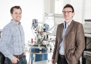
Menno Veldhorst (left in the photo) was lead author of the paper and Professor Andrew Dzurak (right) lead the project. Other UNSW contributors include Henry Yang and Andrea Morello – who leads the quantum spin control research team. Professor Kohei Itoh from Keio University in Japan provided special silicon wafers.

Quantum computers

In classical computers, data is rendered as binary bits, which are always in one of two states: 0 or 1.

A quantum bit (‘qubit’) can exist in both of these states at once – known as a superposition.

A qubit operation exploits this quantum weirdness by allowing many computations to be performed in parallel. According to UNSW, a two-qubit system performs the operation on four values, a three-qubit system on eight, and so on.

“If quantum computers are to become a reality, the ability to conduct one- and two-qubit calculations are essential,” said Dzurak, who jointly led the 2012 team that demonstrated the first ever silicon qubit, also reported in Nature.

In the gate, data is encoded as spin up or spin down – or the superposition of both.

Silicon electron spins have a usable coherence times’, after which data decays to randomness.

In 1998, according to the University, former UNSW researcher Bruce Kane first proposed the idea of using silicon as a base material for quantum computing. In Nature he outlined a silicon-based computer in which single phosphorus atoms in otherwise pure silicon define the qubits.

In 2012 Dzurak and Morello led a team that demonstrated a spin qubit in silicon, but in an atom rather than a transistor.

Last year Dzurak’s team discovered a way to create a qubit with a device similar to a mosfet.

Photo: Menno Veldhorst (left) and project leader Andrew Dzurak in the UNSW laboratory where the experiments were performed.

steve bush

Freescale aims ABS chip at motorbikes

Freescale SB0400 SB0401Motorcycles get their own anti-lock braking (ABS) chip with Freescale’s MC33SB0400 analogue chip, which includes solenoid power stages, but needs no heatsink.

“Introduction of the products coincides with the upcoming initial implementation of European Commission legislation making the fitment with ABS for all new motorcycles above 125cc to be mandatory beginning 1 January 2016,” said Freescale. “By incorporating these 7x7mm devices into their designs, manufacturers of ECUs [electronic control units] no longer must rely on larger ABS ICs developed for automobiles.”

SB0400 works on both wheel, while for scooters and lighter motorcycles there is the one-wheel-only SB0401.

Made on Freescale’s Smartmos mixed signal process, the devices integrate: wheel speed sensor interface, valve drivers (four or two), motor pump driver, safety switch, watchdog and safety state machine; plus protection and diagnostics for: over-voltage, under-voltage, over-temperature, shorted load and open load. An internal charge pump allows n-channel external mosfets to be used to control the pump and isolate the solenoids.

Freescale SB0400 SB0401 appInformation interfaces include: vehicle speed output, warning lamp driver (14Ω), ISO K-line interface for connection to a plug-in diagnostic tester and 16bit SPI serial bus.

Solenoid drivers are rated at up to 5A (160mΩ switch) with PWM up to 5kHz. The pump motor pre-driver works up to 500Hz.

The firm’s functional safety programme (Freescale Safe Assure) is available to help system manufacturers with system compliance with functional safety standards ISO 26262 and IEC 61508. www.freescale.com/SafeAssure.

Both ICs are in volume production.

The MC33SB0400 demo board video is a good introduction and not just fluff. Access to the data sheet requires a log-in, although a cut-down version is freely available.

Freescale aims ABS chip at motorbikes - SB0400 SB0401

Freescale aims ABS chip at motorbikes – SB0400 SB0401

steve bush