Author Archives: richard wilson

Dyson is on fast electronics trajectory

 From being a small part of the traditional vacuum cleaner to defining the product itself with the latest robotic vacuum cleaner, Dyson is placing electronics at the heart of its product development plans.

As a result the consumer products company is dramatically expanding its electronics hardware and software development teams and it is building a new R&D centre in the UK to support the growing electronics design activity.

Dyson is a global brand which has reputation of innovating domestic vacuum cleaner design.

There was not much electronics in the original vacuum cleaners. As a result electronics design played a minor role in the development of the first Dyson products.

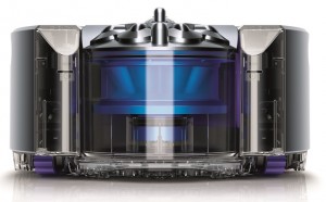
But all this has changed in 2015 with the launch of the Dyson 360 Eye robot vacuum cleaner. Electronics is not only part of the design; electronics defines the product.

Dyson is one of the companies planning to use artificial intelligence and robotics to bring a new level of intelligent computing to the home.

“We have the mechanical and software capabilities, but we still lack understanding – machines that see and think in the way that we do. Mastering this will make our lives easier and lead to previously unthinkable technologies,” says company founder, Sir James Dyson.

Electronics hardware and software design has become an important element in product development at Dyson.

So much so that the company is planning to create a new electronics development centre at its facility in Wiltshire, and the consumer company has a programme to expand its electronics hardware and software development teams significantly this year.

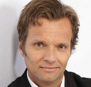
“If we look back at Dyson products over the last 20 years, there was not a lot of electronics in the early vacuum cleaners,” points out Claudio Zizzo global head of electronics at Dyson.

This changed with newer products such as the company’s cooling and heating fans.

“Electronic systems were incorporated for advanced motor control to optimise energy consumption and reduce motor acoustic noise,” explains Zizzo.

“Sir James Dyson was quick to recognise that electronics was no longer just an enabler within the product. With the 360 Eye robot, it is the product,” says Zizzo.

Claudio Zizzo

Claudio Zizzo

Zizzo, who has strong background in managing electronics design groups at Motorola and Rolls-Royce, was recruited by Dyson almost two years ago to build up the firm’s team of electronics hardware, system and software development engineers.

“The company recognised that electronics was becoming a core element of future product development plans,” says Zizzo.

Dyson is making a major investment to expand its electronics development capabilities.

“In the consumer world the pace of development is very aggressive. Dyson is developing electronics technology on a very fast trajectory and we see a big opportunity to innovate,” says Zizzo.

A new robotics laboratory, which the company is building at its Wiltshire headquarters will open in next two months. The company is in the middle of a recruitment programme which will add hardware, software and systems engineers to its development teams.

Dyson has recruited 60 electronics development engineers in the UK in the last 12 months and Zizzo says there are plans recruit another 70 engineers this year.

The company is looking for engineers with a range of skills and experience. “We are looking for graduate engineers, but also experienced engineers and team leaders,” says Zizzo.

Dyson has also collaborated with Imperial College in the creation of a robotics R&D laboratory at the London university.

With research at the Dyson Robotics Laboratory at Imperial College London, which represents a £5m collaboration between the College and the manufacturer, Dyson is looking to apply the operation of robots beyond controlled environments, such as assembly lines where they work within a strict set of parameters.

The idea is that robots could successfully navigate the real world by interacting safely with their surroundings. To do this it is necessary to develop robots that can process visual information in real-time.

The Dyson 360 Eye has a 360 degree camera and many tens of sensors which are used to model the robot’s environment in 3D. 
The goal is for robots not only to determine the layout of a room, but also distinguish between objects and determine their purpose.

Each house is different, points out Zizzo, so the robot must carry out probabilistic and heuristic analysis of the images and sensor data in real-time, which requires high performance digital signal processing and sophisticated software algorithms.

“A lot of learning takes place in the robot with the aim of getting maximum floor/area coverage with the minimum run time,” says Zizzo.

The electronics design activities within Dyson incorporate analogue and power circuit design as well as embedded processor systems design. There is advanced motor control for the four drive motors in each robot, for example as well as radio frequency circuit design for the Wi-Fi system.

Dyson is also developing its own software to control and operate the robot. The software development team numbers 55 people and is growing rapidly.

The software and connectivity team is also responsible for the development of the smartphone apps which are used to operate the robot.

The company which has expanded its horizons from vacuum cleaner design to robotics is not planning to stop looking for new areas in which it can innovate.

Last November, Dyson announced its plans for a £1.5bn investment for future technologies, including a £1bn for the research and development of new product technologies.

Zizzo believes electronics design will become a major element of future product development at the company.

“The products that come after this first robot will have even greater levels of electronics within them,” says Zizzo.
“There is an electronics revolution taking place at Dyson,” says Zizzo. “I believe that anyone joining the company now is joining Dyson at a very exciting point in time.”

Richard Wilson

Linear Tech CEO: industrial market growth “relentless”

Lothar Maier

Lothar Maier

Over the past year, we continued our focus on the automotive, industrial and communications markets. We addressed each with analogue and power solutions to help our customers get to market faster and more reliably.

In the automotive market, fuel efficiency, comfort, navigation/entertainment, and safety drive the need for new analogue solutions.

Many of the mechanical functions in an automobile are being converted to electronic to reduce weight, improve fuel economy and increase reliability. The recent introductions by nearly every automobile manufacturer of hybrid and electric vehicles highlight this trend, and show how electronics are reshaping the automotive market.

The transportation market is our second largest end market, as well as the company’s fastest growing market.

Our largest market is industrial and its growth is relentlessly driven by the need for ongoing innovation.

Our industrial efforts span factory automation and process control, scientific instrumentation, medical and security, among others.

This market demands better efficiency, more automation, greater precision and higher integration, a cycle that started 10 years ago and today shows no signs of slowing.

Looking to the year ahead, I am encouraged that our customers in UK, Europe and other parts of the world continue to seek new design solutions.

I continue to be optimistic about the opportunities in the year ahead.

Lothar Maier, CEO, Linear Technology  

Richard Wilson

Sebastian Conran takes 3D printing into schools

Sebastian Conran

Sebastian Conran

Sebastian Conran has teamed up with publisher, Eaglemoss to bring 3D printing and design into the school classroom.

The Vector 3 printer comes with a step-by-step 3D design tutorial course for school learning.

Sebastian Conran, founding director of Sebastian Conran Associates, said: “As 3D printing technology and applications become more mainstream, 3D printers are moving from the hi-tech workshop into schools, the home and the office.”

Using the Vector 3 in conjunction with the software course will allow students to create a range of objects, including models for science subjects such as cells and molecules.

Maggie Calmels, senior v-p at Eaglemoss, believes that 3D printing allows for a new and “creative approach to teach STEM and design subjects and it is great to be amongst those that are paving the way in making 3D printing available to a wider audience.”

To assist schools with purchasing the product, Eaglemoss has developed a multi printer pack of up to six printers specifically for schools’ supply, plus a schools retail pack of one printer which comes with associated design projects and easy to follow 3D design course for in classroom teaching.

A dedicated website area has also been set up for schools.*

Eaglemoss has also launched the 3D printer as a partwork collection which can be built in weekly installments.

The company is also setting up a 3D design competition for students which will be judged at the Design Museum in June 2015. Prizes include a Vector 3 printer as well as a donation to the winning school’s technology budget.

Richard Wilson

Comment: Product-centric design is the right approach

Bob Potock

Bob Potock

For as long as many of us can remember, the PCB has been at the centre of the product design process.

This PCB-centric design approach is characterised by PCB, mechanical and supply chain teams working in silos until the all the pieces come together at the prototype stage. If something doesn’t fit or a cost target is missed, recovery is expensive.

It’s an approach that has worked reasonably well over the years; but product composition is changing and 2014 saw a marked shift to a product-centric design approach that I expect to see a lot more of in 2015.

Let’s consider system-on-chip (SoC) ecosystems and product packaging. The SoC has had a profound impact on the hardware design process.

With so many functions being consolidated on a single chip and application specific flavours of the SoC, engineers can make use of reference designs. Many products use SoC reference designs with an added special sauce for differentiation.

Product packaging or form factor, on the other hand, has become an important competitive factor and we’re seeing ever more complex shapes and angles.

Consumers are looking for smaller and cooler looking products. This translates into smaller PCBs fitting into smaller enclosures with less room for error.

On one hand, SoC-based reference designs make the hardware design process easier, but those designs still need to fit within a very creative enclosure demanding much closer collaboration between design disciplines.

For example, the enclosure may dictate a two-PCB implementation versus a single board design. Such PCB planning is intrinsic to product-centric design.

This is a big task for current-generation, single PCB 2D design tools. Their limitations include the lack of product-level design visualisation; lack of multi-board support; and limited or no MCAD co-design capabilities, concurrent design support, or cost and weight target analysis.

A multi-disciplinary and collaborative product-centric design process is a profoundly different approach. This is being driven by changing competitive factors and a PCB-centric methodology simply can’t keep up. This changing environment requires a more collaborative and responsive design process.

One key product-centric design feature that allows companies to quickly respond to new and complex product requirements is architectural validation. This is the bridge between the product requirements and detailed design – and it’s an area where companies can achieve a competitive edge for their products if they get it right.

Before detailed design, a multi-discipline analysis of the requirements versus the proposed product architecture is done.

Factors are reviewed such as: size, weight, cost, shape and functionality of the new product; how many PCBs are needed and whether they’ll fit in the enclosure.

Other reasons manufacturers are achieving cost and time savings with product-centric design include:

  • Concurrent 2D/3D multi-board design planning and implementation
  • Import/export of STEP models with clearance and collision checking
  • The use of modular design (design reuse)
  • Improved communication with the supply chain

These capabilities support product-level considerations and enable companies to maximise their competitive edge.

Writer is Bob Potock, vice president of marketing, Zuken.


Richard Wilson

Will 2015 be the key year for graphene?

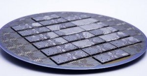
imec wafer scalingGraphene has yet to move out of the research lab, but 2015 could be the year we see the first devices using the “new” semiconductor material.

Imec has developed the industry’s first integrated graphene optical electro-absorption modulator (EAM) capable of 10Gbit/s modulation speed with a very low insertion loss and drive voltage.

For chip-level optical interconnects, graphene will be used for its fast tunable absorption over a wide spectral range.

Imec is also developing a scalable, manufacturable silicon-based optical interconnect technology for telecoms applications.
Researchers at IBM have used graphene in a re-usable substrate for making blue LEDs.

“In principle, graphene has been demonstrated as an infinitive source for growing these [GaN] semiconductor materials, making the work an enormously cost-effective and reliable production method for single-crystalline films,” said IBM scientist Dr Jeehwan Kim.

“Growth of a 4 inch, wafer-scale GaN film would require a 4-inch SiC wafer at the cost of some $3,000. Now, graphene can be produced in a lab to replace the expensive SiC wafer,” said Kim.

Graphene NanoChem, the Malaysia-based graphene company, has announced a product development agreement with Sync R&D for graphene-enhanced lithium-ion batteries for use in electric buses

The Li-ion battery is anticipated to be a critical component for electric vehicles as a fully charged battery will enable the bus to travel between 180 and 200km before requiring to be recharged.

A graphene-enhanced anode in the Li-ion battery is claimed to provide 10 times more power storage and significantly reduces the time required to recharge the battery.

Richard Wilson

Comment: let’s move chip design a little to the left

Untitled

Alex Duesener

Looking ahead to 2015 in the electronics industry, I see a shift left.

To explain, let me back up a bit. Whether it’s the automotive electronics segment, the internet of things (IoT), or mobile devices, the consumer now dictates design in a way he or she hasn’t historically.

Consumers of electronics technology now expect amazing new functionality each year, because we’ve delivered stunning electronics innovation for decades.

This has changed the nature of system design forever. The slow evolution away from partitioned design tasks and siloed teams has made the jump to hyper drive as design shifts left.

The Shift Left

What does this mean? Simply put, everything that was done “later” in the design flow must now start “earlier.” Software development needs to begin early enough to contemplate hardware changes (i.e., hardware optimization and hardware-dependent software optimization), while at the other end of the spectrum we see very early collaboration between foundries, electronic design automation (EDA) tool providers, and intellectual property (IP) suppliers to “co-optimize” the value proposition of each new process node.

This evolution’s essence is the examination of any and all dependencies in the product planning and development process to understand how they can be made to overlap in time.

Early software development helps enable software-driven verification methodologies. In turn, these methodologies are used to verify that the integration of sub-systems does not break the design, and that performance and energy can be optimized in the system context, with both hardware and software optimizations possible.

Numerous design processes are shifting left, but let’s take just one as an example: High-performance mixed-signal IP, such as DDR4 PHY in 16nm/14nm FinFET technologies, needs to be proven early in the process decision lifecycle. For this reason, foundries, EDA companies, and IP providers collaborate to make sure that critical IP blocks that will be needed by the first wave of process adopters are on early shuttle test chips.

Integration, Verification Evolution

The shift left also creates the need for faster subsystem integration and assembly along with retargeting of existing subsystems, the prototyping of new ones, along with performance, power, and area (PPA) analysis.

There are key changes in hardware verification too. The trend towards metrics-driven verification closure and unified verification methodology (UVM) continues proliferating at an accelerated pace. Verification IP (VIP) plays a critical role, in providing proxies for incomplete aspects of the system, as well as in proving adherence to interface standards.

While simulation remains the main workhorse for IP and subsystem verification, emulation has taken centre stage for system-on-chip (SoC) hardware verification, hardware/software integration, and operating system (OS) bring-up. Specialized hardware for emulation, acceleration, and prototyping is being applied by a much broader set of design teams to accelerate regressions and open the door to software-driven hardware verification methodologies.

In summary, the simultaneous and interrelated drives for faster time to market, product differentiation, and profit will all drive big changes in the way that electronics products will be designed in 2015 and beyond. Design teams shifting to the left will be the ones to reap big rewards and dominant shares in their markets as they do so.

Writer is Alex Duesener, corporate vice president for EMEA with Cadence.

richard wilson

Comment: Energy harvesting will be big in 2015

Dr. Wald Siskens, CEO of EnOcean

Energy is within reach everywhere, it just needs to be harvested: this is the principle of energy harvesting. Energy harvesting wireless solutions are already well established in the commercial building automation sector and for smart home systems. However, the technology is just getting started.

In 2015, new application fields for batteryless wireless communication will emerge to further enhance the world around us.

The “Forget Me Not” challenge at the end of 2014, a global design competition organised by the element14 community, gave us a taste of the technology’s possibilities. Engineers from around the world applied with their ideas for pioneering applications in the field of wireless monitoring and automation to perform tasks in our modern lives.

The projects included everything from a smart home security system to technology allowing users to take care of their pet remotely, to a system telling them if they’ve left laundry in the washing machine or to providing assistance systems for elderly people.

Most of these engineers were designing with energy harvesting wireless technology for the first time and this was no hurdle at all. On the contrary, the possibilities of sensors gaining their energy from the surrounding environment inspired many new ideas.

The flexibility of self-powering made the designers think about placing sensors in areas where data collecting devices that need maintenance or cables are not an option – a key parameter for the internet of things.

Powering sensors from the surrounding environment is not just a cool technology, it also ensures there is never any interruption in data collection needed to improve the interaction with our world.

Collecting and processing data opens up new possibilities for organising our daily lives independently from location and time. Thereby, data, collected once, can be reused for several applications. In a house, for example, the same system that saves energy based on the current room temperature, humidity, presence of persons and weather data also ensures a healthy comfort for the tenants or more security at home.

Batteryless sensors and switches are the assistants we need to collect and transmit the data. The tiny devices are indispensable for machine-to-machine communication, for efficient use of resources, for optimised sustainable agriculture or for demand-driven energy distribution.

Intelligent sensors, which monitor bridges, skyscrapers or dams, will lead to better sustainability of our constructions and save costs for future generations.

The intelligence to make use of the data can and will be implemented anywhere, but the systems that collect the initial information need to be reliable and perpetual so that we can “install and forget” this is where energy harvesting wireless sensors come in: the “things” in the IoT.

Writer is Dr. Wald Siskens, CEO of EnOcean

richard wilson

Top 10 technologies to transform the world

IoT (Photo: Intel)

IoT (Photo: Intel)

Cloud computing/big data and 3D printing and (of course), the internet of things (IoT) are the three technologies most likely to transform the world during the next five years, according to technology market analyst IHS Technology.

These are the technologies which could change the world the Gutenberg printing press to the steam engine to the microchip.

So IHS Technology gathered its experts representing the technology supply chain from electronic components to finished products across applications markets ranging from consumer, media, and telecom; to industrial, medical, and power and them asked to nominate and vote for their top 10 most impactful technologies over the next five years.

The top three technologies were: 3D printing in third place, cloud computing/big data at No. 2, and little surprise that IoT comes out on top.

Total revenue for the 3D printing industry is forecast to grow by nearly 40% annually through 2020, when the aggregated market size is expected to exceed $35bn, up from $5.6bn in 2014.

IHS forecasts that global enterprise IT spending on cloud-based architectures will double to approximately $230bn in 2017, up from about $115bn in 2012.

The potential of IoT replies on predictions that more than 80 billion Internet-connected devices are projected to be in use in 2024, up from less than 20 billion in 2014.

The other key technologies identified by IHS Technology analysts were:

  • Artificial intelligence
  • Biometrics
  • Flexible displays
  • Sensors
  • Advanced user interfaces
  • Graphene
  • Energy storage and advanced battery technologies


richard wilson

ARM challenges young engineers in California

logoARM has partnered with the Tech Museum of Innovation in San Jose, California to sponsor a video contest for the Tech Challenge 2015.

The contest is open to boys and girls in grades 4-12 to make a video of how they tack real-world problems using engineering-design thinking.

The annual two-day event tests skills such as creativity, problem-solving and design. It also helps participants to deal with risk-taking and teaches them how to learn from failure and perseverance.

This year’s challenge, which takes place on April 25 & 26, is to build an earthquake-safe structure.

Videos may record the design brainstorming process or simply chart the project as a whole. The films will be judged on creativity, visual and audio appeal and storytelling. The top three videos will receive an award and be played during the event.

Where: The Tech Museum, 201 South Market Street, San Jose, Calif., 95113

When: Contest final dates:

· Saturday April 25, 2015, Grades 4-6 and 9-12

· Sunday April 26, 2015, Grades 7-8.

The Tech Challenge 2015


richard wilson

Power efficiency is the universal design challenge of the decade

Mark Downing

Mark Downing

Power efficiency has been the most pressing and universal design challenge for the last decade, and that pressure in this area of system design is only increasing.

We all know the reasons why: We are trying as a planet to reduce our energy demands, while looking for “greener” approaches to many of our most power hungry applications. This is driving regulation that impacts a number of telecommunications, industrial and consumer electronics.

We are reliant on mobile technologies for communication, data aggregation, and entertainment, and these technologies have increasing functionality in a smaller and thinner footprint. This constrains the size of the battery and requires further innovation to enable us to keep these mobile devices unplugged.

The infrastructure being built to support the massive increase in data transmission and storage is itself a big energy drain, costing more to cool than the equipment itself. There are a couple of key areas where silicon providers can innovate to make a difference in power efficiency.

Power efficiency is critical to attaining the performance for demanding processor, FPGA and memory loads, and critical to extending battery life in portable products. To address these power challenges, we are focused on the key areas — buck-boost regulation, processor core power, and display and backlight drivers — where silicon providers can innovate to make a difference.

In 2015 and beyond, preserving or extending battery life will be a key challenge.

Cloud computing is also increasing the demand on our computing infrastructure, with industry experts forecasting global data center IP traffic growth at a compound annual growth rate of 25% through 2017. These data centres are struggling to keep pace with electricity demand. Server and enterprise storage platforms are increasing the number of voltage rails, and adding complexity that will require a much higher level of system intelligence to enable efficiency and fault management.

Higher system power densities must also be achieved to preserve precious real estate and reduce system cost. Given these dynamics, 2015 will be an exceptional growth year for digital power due to its lower cost and ease of use.

From our perspective, the ongoing delivery of capabilities that can provide both the incremental improvement and leapfrog efficiency gains that enable customers to achieve, and then exceed their power goals is what’s driving the semiconductor industry.

Writer is Mark Downing, senior vice president, strategy and infrastructure/industrial power products, Intersil


richard wilson