Author Archives: richard wilson

STMicroelectronics researches potential of FD-SOI for high-rel

STMicroelectronics Crolles fab in France

STMicroelectronics Crolles fab in France

STMicroelectronics is working with the French universities to create a high-reliability semiconductor research laboratory.

The Radiation Effects and Electrical Reliability (REER) Joint Laboratory is a multi-site research establishment that will bring together teams from the IM2NP Institute, based in Marseille and Toulon, and specialist engineers from the ST facility in Crolles, near Grenoble.

The REER Joint Laboratory’s research will focus on two main areas of research: the effect of radiation on the 28nm technology node and beyond, in particular the FD-SOI (fully depleted silicon-on-insulator) industrial cluster developed by ST at its Crolles site.

This research is applicable for sectors, such as the space but also high growth sectors like automotive, medical and security.

“For these types of applications, the intrinsic constraints of electronic components (electrical fields, mechanical stress, temperature, etc.) and some environmental constraints (especially particle radiation from natural or artificial sources) are becoming an increasingly critical issue for current and future generations of integrated circuits,” said the group.

The lab will also be involved with collaborative programmes and projects at the national, European and international level, in conjunction with the European CATRENE cluster, the ENIAC initiative and support programs led by the French General Directorate for Enterprises (DGE) and the French defense procurement agency (DGA).


Richard Wilson

Graphene-based film can super cool LEDs

UntitledResearchers at Chalmers University of Technology have developed a method for efficiently cooling electronics using graphene-based film.

According to the researchers, the graphene film has a thermal conductivity capacity that is four times that of copper.

Significantly the team has developed a graphene film that  can be attached to silicon substrates.

Research team leader Johan Liu, professor at Chalmers University of Technology, writes:

“But the methods that have been in place so far have presented the researchers with problems and it has become evident that those methods cannot be used to rid electronic devices off great amounts of heat, because they have consisted only of a few layers of thermal conductive atoms.

“When you try to add more layers of graphene, another problem arises, a problem with adhesiveness. After having increased the amount of layers, the graphene no longer will adhere to the surface, since the adhesion is held together only by weak van der Waals bonds.”

“We have now solved this problem by managing to create strong covalent bonds between the graphene film and the surface, which is an electronic component made of silicon,” he continues.

The stronger bonds result from so-called functionalisation of the graphene, i.e. the addition of a property-altering molecule. Having tested several different additives, the Chalmers researchers concluded that an addition of (3-Aminopropyl) triethoxysilane (APTES) molecules has the most desired effect.

When heated and put through hydrolysis, it creates so-called silane bonds between the graphene and the electronic component (see picture).

The researchers have shown that the in-plane thermal conductivity of the graphene-based film, with 20 micrometer thickness, can reach a thermal conductivity value of 1600 W/mK, which is four times that of copper.

A likely application says Johan Liu is the integration of graphene-based film into LEDs, lasers and radio frequency components for cooling purposes.


Richard Wilson

Wireless will replace wires, says Bell Labs chief

Marcus Weldon, CTO Bell Labs

Marcus Weldon, CTO Bell Labs

Phones lines to homes and offices will one day be defunct and we will all one day connect to telecoms networks wirelessly, according to Marcus Weldon, president of Bell Labs and CTO of Alcatel-Lucent.

He also believes networks will be rebuilding themselves like connections in the human brain to meet the enormous demand for data communications.

Weldon, who presides over research at Bell Labs, which looks at technology that will have an impact in five years, believes that the last few metres of communications networks will eventually be wireless – to fixed locations as well as to mobiles.

“The default way of connecting will be wireless in the last 10 to 100 metres,” said Weldon.

Behind the wireless networks will be optical and wireline networks with enormous data capacity.

But Weldon believes the data centre and intelligence in this network will move closer to the edge of the network, and will be closer to the user to be more responsive.

“The network will be not be a single ‘cloud’ but will be built from ‘edge clouds’ connected by small wireline networks of very large capacity – these will be copper cabling or optical fibre,” said Weldon.

Building these networks will be challenging for the industry, but Weldon believes the biggest challenge the communication industry faces in the next five years is in the wireless access network.

“The biggest technical problem is in the wireless domain,”he said.

The inherently “unguided” nature of wireless communications makes it susceptible to interference and reflections.

“As a result, to get the capacity we will need will be a big challenge,” said Weldon.

The answer, he said, is to make the networks more agile and responsive to change.

“The IoT will soon be upon us and this will need a ‘living network’,” said Weldon.

“This will involve analysing how people move and this data will be used to optimise the network. The network will constantly be reconfiguring like the synapses in the human brain,” he said. And he expects to see this happening by 2020.

Richard Wilson

Nasa plans to send CubeSats to explore planets

Nasa/Goddard-MIRCA-Cubesat

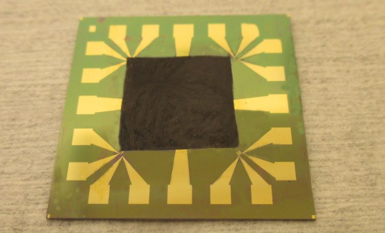
The miniature prototype entry vehicle for interplanetary exploration, called the Micro-Reentry Capsule (MIRCA)
Source: NASA/Goddard

Low cost miniature satellites could one day be used to orbit and explore distant objects such as planets and comets.

Nasa is investigating the feasibility of sending CubeSats out of earth orbit to investigate distant objects.

The hope is that this will dramatically reduce the cost of sending probes to investigate such objects as Comet 67P/Churyumov-Gerasimenko, which has been explored by the Rosetta mission. Rosseta’s comet lander, called Philae, is the size of a large domestic appliance. CubeSats, by contrast, are about the size of a loaf of bread.

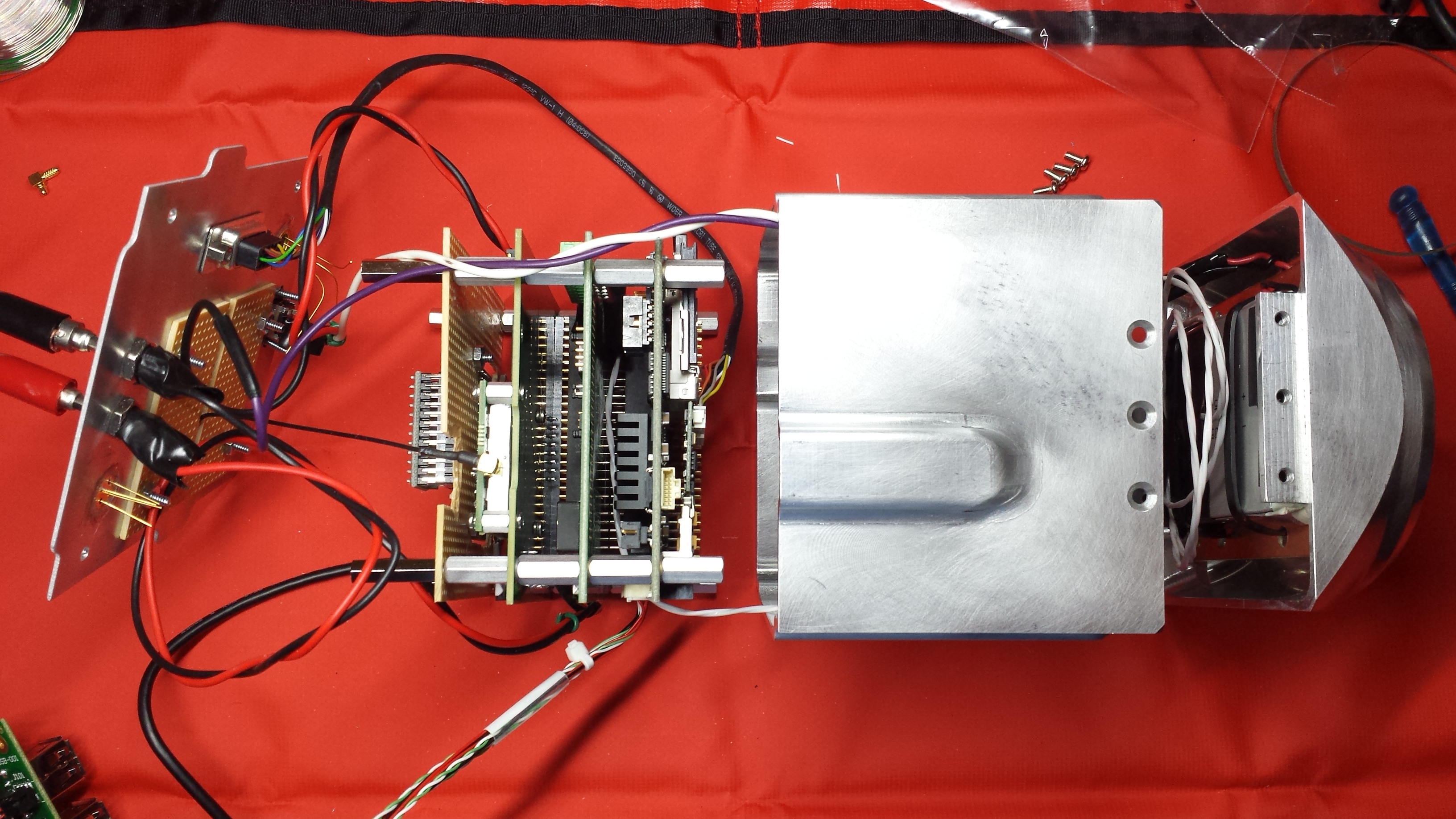
Jaime Esper and his team at Nasa’s Goddard Space Flight Center in Maryland are planning to test the stability of a prototype entry vehicle, the Micro Re-entry Capsule (MIRCA), this summer during a high-altitude balloon mission.

Planetary missions

Dubbed the CubeSat Application for Planetary Entry Missions (Cape), the concept involves the development of two modules: a service module that would propel the spacecraft to its celestial target and a separate planetary entry probe, which could survive a rapid dive through the atmosphere of another planet, all while transmitting scientific and engineering data back to Earth.

“The Cape/MIRCA concept is like no other CubeSat mission,” Esper said. “It goes the extra step in delivering a complete spacecraft for carrying out scientific investigations. We are the only researchers working on a concept like this.”

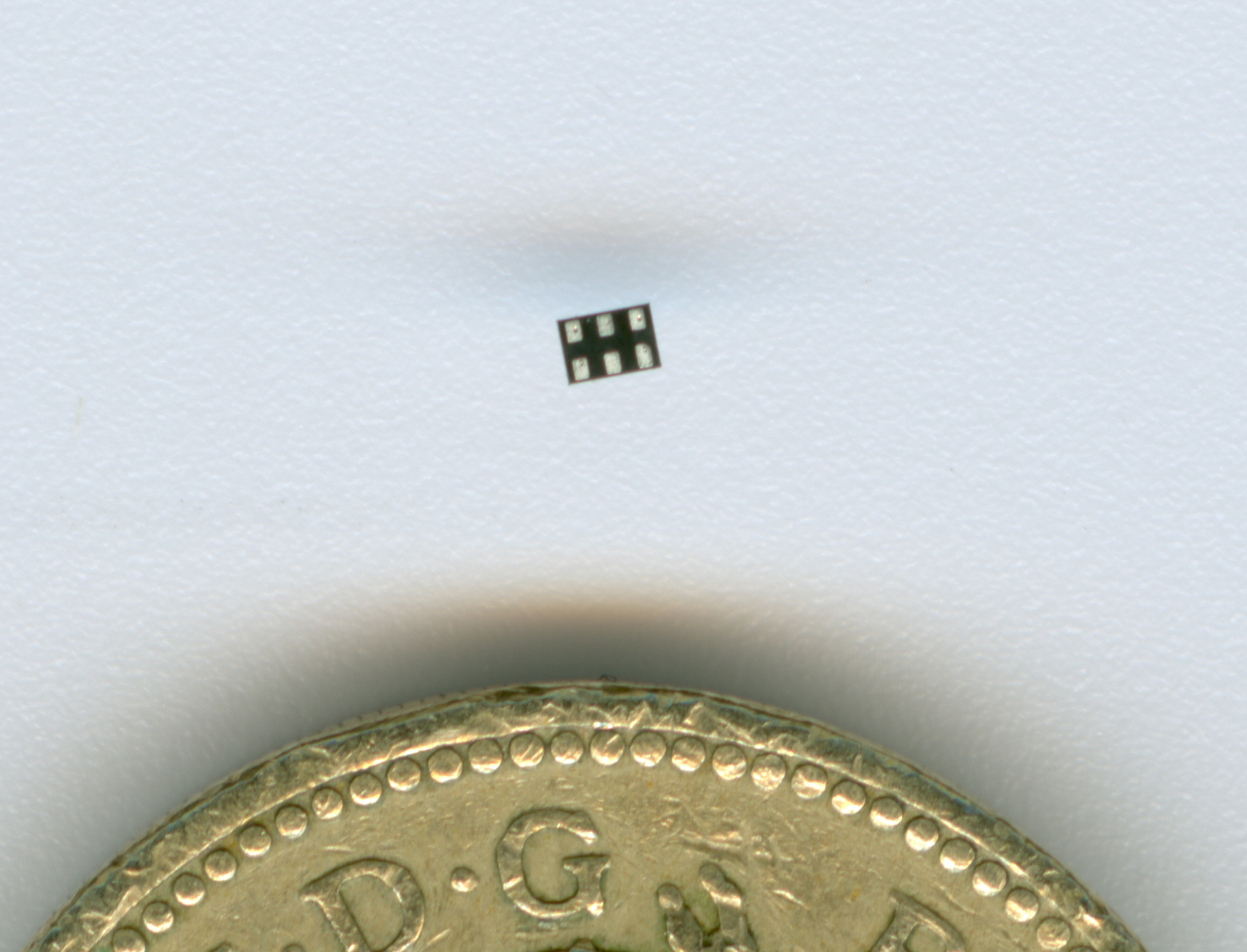
The Cape/MIRCA spacecraft, including the service module and entry probe, will weigh less than 4.9Kg and have dimensions of 10cm³.

cubesat-WEB-NASA

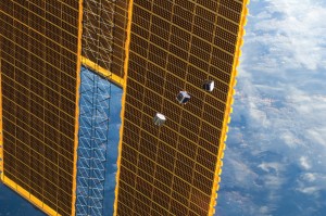
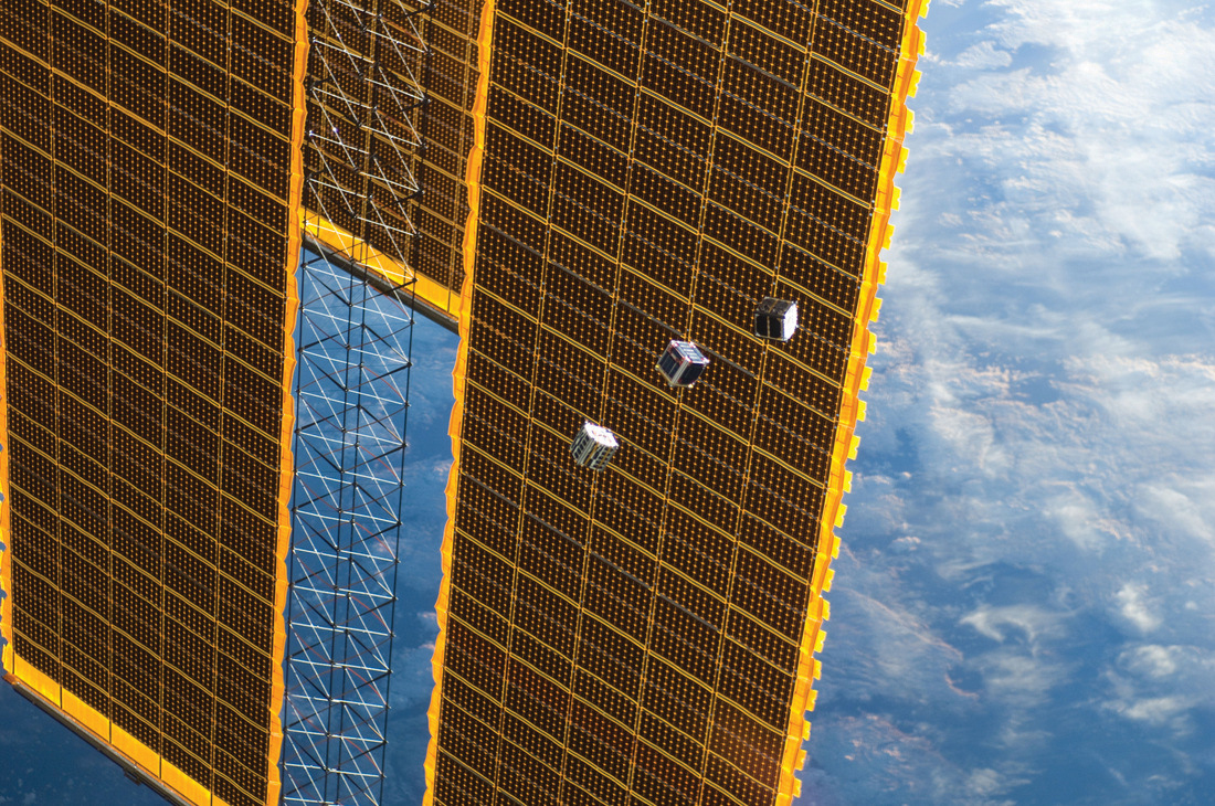
CubeSats being released from the International Space Station in an earlier mission

It would be ejected from a canister housed on its mother ship and would have its own solar panels to power it on its journey to another planetary body.

Once it reached its destination, the sensor-loaded entry vehicle would separate from its service module and begin its descent through the target’s atmosphere.

It would communicate data about atmospheric pressure, temperature, and composition data to the mother ship, which then would transmit the information back to Earth.

Multi-point sampling

The attraction is that cubesats are relatively inexpensive to build and deploy, scientists could conceivably launch multiple spacecraft for multi‑point sampling – a capability currently not available with single planetary probes that are the Nasa norm today, said Esper.

So the first step is demonstrating a prototype of the MIRCA design during a balloon mission this summer.

According to the plan, the capsule, manufactured at Nasa’s Wallops Flight Facility on Virginia’s Eastern Shore, would be dropped from a balloon gondola at an altitude of about 30km to test the design’s aerodynamic stability and operational concept.

During its free fall, MIRCA is expected to reach speeds of up to Mach 1, roughly the speed of sound.

“If I can demonstrate the entry vehicle, I then could attract potential partners to provide the rest of the vehicle,” said Esper.

The next step, says Esper, may be to drop the entry vehicle from the International Space Station, perhaps as early as 2016.

This would expose the capsule to spaceflight and the heat of atmosphere re-entry.

Richard Wilson

Arduino shrunk for wearables

Arduino Gemma

Arduino Gemma

There is now a slimmed down version of the Arduino embedded system development platform which has been down-sized for use in wearable and IoT applications.

The Arduino Gemma is a miniature wearable device board based on the ATtiny85 microcontroller.

ATtiny85 is Atmel’s 8-bit AVR Risc-based microcontroller with 8kbyte ISP flash memory, 512byte EEPROM and 512byte SRAM.

The MCU achieves a throughput of 20MIPS at 20MHz and operates between 2.7-5.5V.

The board has three digital input/output pins. Two of these can be configured as PWM outputs and the other as an analogue input.

It sells for $10 in the US.

On the board are an 8MHz resonator, a micro USB connector, a JST connector for a 3.7V Li-Ion battery and a reset button.

It can be powered via the USB cable or a battery.


Richard Wilson

Micro-pump in the eye could treat glaucoma

Cross-section of the eye with the implant

Cross-section of the eye with the implant

Researchers are developing an implantable microfluid system which they claim can stabilise intraocular pressure in the human eye, a condition which can impair sight.

Researchers at the Fraunhofer Research Institution for Microsysems and Modular Solid State Technologies EMFT are working on a  way to treat diseases of the eye such as glaucoma and phthisis bulbi with an active implant that is intended to regulate eye pressure.

“This way, we can spare the patient from the strain of multiple follow-up procedures, and can preserve the ability to see over a longer timeframe and, in the best case scenario, completely prevent blindness,” said Christoph Jenke, project manager at EMFT.

The implant consists of a micro-pump system, a sensor-based pump control, an integrated battery for solid state energy supply as well as a telemetry module for data transmission. It can be attached directly to the eyeball.

The Munich-based researchers developed a biocompatible silicon micro-membrane pump, measuring 7x7x1 cubic mm, with a production rate of 30 microlitres per second.

Depending on the disease, it can moisturize the eye or drain intraocular fluid.

Fraunhofer experts use the eye’s natural drainage pathways so that no scar tissue forms. Monitoring at regular intervals, based on a conventional eye pressure measurement ,the attending physician can set the volume of fluid to the desired level on an outpatient basis.

There are also plans call to combine the system with an implantable sensor, so that fluids can be regulated automatically.

“Our implant imitates a healthy eye’s natural production of cameral fluid. Since the absence of vitreous humor production is the exclusive cause of the disease in phthisis, we are optimistic that we can stop the disease progression and be able to preserve the eyesight sustainably,” said Jenke.

The team is building a demonstration system which will be used for reliability and lifecycle testing.

The work, which also includes Geuder AG, is being carried out as part of the Microaug project, under the KMU Innovativ Program sponsored by the German ministry for education and research.

Richard Wilson

Qt moves into the world of IoT

Qt-logoIoT is a new focus for the Qt mobile development environment which works cross-platform which now incorporates Bluetooth Low Energy (Bluetooth Smart).

It can be used to write cross-platform code for communicating with smart sensors, wearables and other BLE-enabled peripherals.

The latest version of the Qt mobile application and user interface development framework also has support for upcoming Windows 10 with full support to come with a subsequent Qt 5.5.x patch release after the final Windows 10 is released.

Qt version 5.5 will allow developers to reuse existing Qt code to build and run on Windows 10.

In another move to support desktop development, Qt 5.5 also supports Red Hat Enterprise Linux 6.6 and will include a pre-built version of Qt for this platform.

There are also two new modules related to 3D graphics development. Qt Canvas 3D provides a WebGL-like API that can be implemented using the Qt Quick UI tool to make loading and displaying 3D content a trivial task.

The Qt 3D 2.0 module, which is included as a technology preview, provides both C++ and QML APIs to simplify the integration of 3D content with Qt applications.

There is better handling of real-time camera feeds and video processing. This includes a video filtering feature that allows the integration of frameworks such as OpenCL and CUDA with VideoOutput elements.

On Linux platforms, gstreamer 1.0 is now used as a default backend.

Qt 5.5 introduces a Qt Location module as a technology preview, adding mapping, geocoding, routing and places support. In conjunction with the existing Qt Positioning API, Qt Location provides everything needed to create location-aware applications. It can make use of a variety of map data providers including Nokia Here, Mapbox and Openstreetmap.


Richard Wilson

Comment: IET “ones to watch” on track to deliver

EPA186In its December 2014 “Ones to Watch” report, the Institute of Engineering and Technology (IET) highlighted six areas that it believed “offer significant promise to the UK and its economy”.

The six technology areas were: new power networks, space, cyber security, additive manufacturing, food security and robotics.

The question is, six months on, how are these industries developing?

Positive results
So far, each one has seen positive results. Research and funding into all of these industries is high, but there is a lack of new commercial output.

The focus in the UK is more on developing new start-up businesses within each industry – to further research vital areas of potential development rather than to compete immediately in each commercial market.

For instance, the UK is currently a European leader in smart grid research, which could pay off in the future as businesses position themselves as market experts.

Meanwhile, in the US, the unveiling of Tesla Motors’ PowerWall and the announcement of Bosch’s DC Microgrid already this year show the global competition faced in new power networks. The UK is not currently a strong commercial competitor in this sector.

Hardware developments
In contrast, in cyber security, the industry hasn’t yet seen any really major developments this year, but the UK remains a world leader.

It’s at the forefront of the industry with many firms partnering with US companies to deliver commercialised products. This is evident in the increasing UK presence at RSA conventions for instance, where exporting skills and services is helping the industry move forward.

That’s not to say that the UK isn’t producing any new physical technology. In the space industry, 2015 has seen the creation of the Mercury Imaging X-Ray Spectrometer (MIXS) – an instrument developed at the University of Leicester for the ESA’s BepiColombo 2017 Mercury mission.

In the robotics industry, Plymouth-based Open Robotics has developed a prosthetic robotic hand using 3D printed materials and, in pure-play additive manufacturing, Renishaw Plc continues to prosper in the global market.

Of course, as the IET itself identified, the volume of engineers and technicians in each industry, as well as their skill-sets, limits the UK’s industrial growth. This remains a challenge that the country must overcome if these six industries are to develop drastically and meet the needs of the future.

As it stands, there has been some development in each industry in the UK, but not yet enough to make a big impact on a global scale. The IET’s Ones to Watch  are steadily growing and developing, with increased interest in start-ups, but none are, truly speaking, the finished article in the international stage.

However, they are all young industries and, if they stay on track, the UK’s knowledge engineering base could allow it to become a serious global technology contender. It’s a golden opportunity but it has to be seized.

Writer is Jonathon Wilkins, Marketing Director for European Automation

Richard Wilson

University embeds RFID chips in yarn

RFID chip and pound coin

RFID chip and pound coin

Researchers at Nottingham Trent University have come up with a way of embedding RFID chips in yarns which can then be woven or knitted to make fabrics for clothing.

Professor Tilak Dias of the Advanced Textiles Research Group of the School of Art & Design, claims that the embedded chips “cannot be seen in situ by the naked eye”.

He has patented the technology, which he believes has the potential to be used for security in stores and also for clothes that are donated to charity to be tracked around the world.

Professor Dias writes:

“If an RFID chip is embedded into a shirt, for instance, it will provide a much greater level of anti-theft and anti-counterfeiting protection. As people will not be able to easily identify where a chip is located in a garment, shoplifters won’t be able to cut it off to steal it.”

Sealed inside resin micro pods within yarns, the fabrics incorporating RFIDs can be run through washing machines and tumble driers without incurring any damage.

Short thin copper strands attached to the either side of the chips are embedded in yarn fibres and act as an antenna.

Measuring one millimetre by 0.5 millimetre in size, when bought in bulk the chips can cost only a few pence each.

Similar to the RFID devices now used in bank cards for contactless payments, the tiny chips can contain all the information which is usually communicated via barcode.

“In relation to recycled clothes, charities would be able to sort garments much quicker – perhaps even in an automated way – to identify the types of clothing that are suitable for different countries according to their requirements,” said Professor Dias.

 Professor Tilak Dias, Stephen Lorimer from Sustainable Society Network+, Dr Colin Cork of Nottingham Trent University and Anura Rathnayake

Professor Tilak Dias, Stephen Lorimer from Sustainable Society Network+, Dr Colin Cork of Nottingham Trent University and Anura Rathnayake

Professor Dias also believes that in the distant future this technology could be used in conjunction with smart washing machines to warn consumers of mixed colours or inappropriate temperatures.

Research fellow Anura Rathnayake, who is involved with the project, added:

“In the long run this technology could be of tremendous benefit to charitable organisations which spend a great deal of time directing donated clothing to people around the world.”

The study was supported by a £50,000 grant from Sustainable Society Network+, as part of the RCUK Digital Economy Theme


Richard Wilson