Author Archives: richard wilson

Atmel adds big data cloud services to IoT chips

atmel-cloud-partners-496x183Atmel is the latest semiconductor supplier to tap into the internet of things (IoT) opportunity with the creation of cloud services to support its MCUs and wireless chips.

A number of partners companies will provide internet-based cloud services for device management and data analytics. These are becoming important elements in IoT design where embedded MCUs and other ICs generate data which is managed by cloud services.

It also creates the potential for remote management of embedded MCUs and controllers in home automation and security monitoring applications.

Atmel expects to add a number of cloud service partners to its ecosystems over the coming months.

Reza Kazerounian, general manager of the microcontroller business at Atmel writes:

“Launching this highly anticipated IoT ecosystem partner program, we are now one of the few suppliers that delivers solutions from the edge node to the cloud, along with full software support.”

Atmel has a range of  pre-certified Wi-Fi, 802.15.4, and multimode modules and MCUs for embedding in IoT nodes and networks.

Access to the application programming interface (API) to qualified cloud partners will be provided through the supplier’s various development boards.

These include the WINC1500-XSTK, SAMW25-XPRO, SAMR21-XPRO and the Arduino Zero.

Richard Wilson

Sheffield-based firm liquid cools HPC networks

Iceotope_cabinetSheffield-based firm Iceotope, which specialises in the liquid cooling of electronic systems, says it has developed a fan-less Mellanox-based InfiniBand and Ethernet network and interconnect switch for supercomputer (HPC) systems.

Mellanox’s low latency switches can be cooled with hot water (of up to 45 deg C), effectively removing the need for forced airflow cooling systems.

Supercomputers which make up high performance computing (HPC) systems typically transmit large amounts of data, with low-performance interconnects often acting as a bottleneck.

Switches lower the energy used by more efficiently switching data transmitted, but to date units have always been cooled by air rather than liquid.

Iceotope founder and chief visionary officer, Peter Hopton said:

“The HPC industry is embracing liquid cooling at a remarkable rate, it’s just a case of technologies being available to match demand. Until now, it was widely accepted that the interconnect switch would never be liquid cooled. It’s great to be able say that, thanks to our work with Mellanox, that’s no longer the case.”

Liquid cooling systems work by transferring all the heat directly into liquid. The waste heat is then removed in the form of hot water, which is pumped around the cabinet and can be re-purposed for domestic heating.

The switches offer Iceotope’s “hot swap clean and dry” user experience, much like a traditional air-cooled server blade, taking up one standard slot on the Iceotope Petagen cabinet (which delivers up to 72 in total).

Switches available include 36 Port – FDR 56Gbit/s InfiniBand and 40/56Gbit Ethernet– with Iceotope looking to support technologies such as EDR 100Gbit/s InfiniBand as part of its development pipeline.

“Liquid cooling is an extremely exciting proposition in the HPC market,” said Gilad Shainer, vice president of marketing at Mellanox Technologies.


Richard Wilson

CEA-Leti demonstrates high density finfets

300mm Coolcube wafer

300mm Coolcube wafer

CEA-Leti has announced first results towards the demonstration of a finfet technology which stacks in 3D active layers of transistors in greater density.

The sequential integration technology called CoolCube can potentially be produced in finfet technology on CEA-Leti’s 300mm production line.

“Key process steps developed on 300mm wafers show progress in closing the gap between the demonstration of a single device and taking the technology to fabrication,” said CEA-Leti.

The process technology has been under development for eight years. It cuts by 50% the thermal budget in manufacturing transistors, while maintaining their performance.

It also allows designers to include backside imagers in the chips, and co-integration of NEMS in a CMOS fabrication process also is possible.

“CoolCube enables local via density that is 10,000 times higher than ‘standard’ 3D integration, because the technology is designed to connect stacked active layers at a nanometric scale,” said Maud Vinet, Leti’s advanced CMOS laboratory manager.

“In the digital area, we expect this 3D technique to allow a gain of 50 percent in area and 30 percent in speed compared to the same technology generation in classic 2D – gains comparable to those expected in the next generation.”

Richard Wilson

Sensor firm expands on back of Watch design-in

AMS Fab B

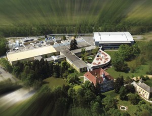
AMS Fab B, top right

Smart sensor firm ams is going from strength to strength.

With a number of high-profile design-ins in the mobile and wearables markets, including the Apple Watch, the Austria-based semiconductor company has expanded is presence in the Asian market.

It has opened a new office in Pangyo, South Korea to address the growing market for mobile and biotech.

This follows the opening of a design centre in Japan.

The company has also recently expanded its chip testing facility in Calamba City, Philippines, in response to growing global sales on the back of the Apple Watch design-in.

According to Jong Duck Lee, Korea country manager of ams, the company will concentrate on providing “more strategic and closer support to our customers as it is recognized as one of  the most cutting-edge and advanced industrial complexes and is located near leading manufacturers in Korea.”

“This demonstrates a commitment to provide continuous investments and efforts in growing the local presence in the region as well as an appreciation of the strategic importance of the Korea market.”

In May, ams announced that automotive equipment supplier Marquardt is using its AS3914 NFC reader IC in a range of contactless door lock and ignition control modules.

Marquardt is a supplier to many big name car manufacturers around the world.

The expansion of the ams chip testing facility in Calamba City means an increase of 130% in size and will result in a total net production area of 10,000m².

The building will test assembled analogue ICs, sensors and sensor interfaces  for the automotive, medical, industrial, and consumer electronics industries.

Thomas Stockmeier, chief operational officer at ams said:

“As a global leader in analogue ICs and sensor solutions, we are proud to have the skill and dedication of our Philippines workforce with currently 500 people and we are excited to see the new investment underlines our confidence in our overall growth strategy.”

This year the firm claimed to have the smallest ambient light sensor which uses through-silicon via (TSV) packaging to achieve a footprint of just 1.145 x 1.66mm and a height of 0.32mm.

The TSV package does not need wire bonds and provides a direct connection from the device I/Os to a solder ball.

According to David Moon, senior marketing manager in the Advanced Optical Solutions division of ams:

“With a footprint of less than 2mm2 and a height of only 0.32mm the TSL2584TSV marks a major milestone in the development of ALS solutions, opening up many new options for implementing display management in highly space-constrained designs.”


Richard Wilson

Nujira shuts with Qualcomm $50m deal reported

nujiraNujira’s life as an independent company seems to have ended.

A report in Business Weekly, which broke the story two weeks ago says that the Cambridge-based developer of mobile power optimisation technology has been bought by US mobile chip giant Qualcomm for $50m.

Nujira’s website has effectively closed down and an unconfirmed report says the CEO and a number of other staff have left the company, which is known to have 200 patents pertaining to the development of envelope tracking technology.

Qualcomm has developed its own envelope tracking (ET) technology, which modulates power levels in the mobile phone’s wireless transceivers.

In November, Qualcomm introduced its second- generation envelope tracking device, the QFE3100.

But if it is confirmed that Qualcomm is the buyer of Nujira then it seems that it values the ET technology which the Cambridge firm has been developing for the last five years.

Nujira was an early pioneer of ET technology, but has struggled to win customers for its ICs among the big players in the mobile phone sector.

It is thought that ET technology from various chip suppliers is being used in smartphones of Samsung, Apple and HTC.

Nujira has not yet confirmed any specific smartphone design-ins.

With envelope tracking, the voltage of the power supply is modulated to follow the envelope of the RF signal passing through the power amplifier (PA) with just enough headroom to keep the PA running smoothly.

This reduces power dissipation in the power amplifier output transistors.

If the envelope tracking power supply is switch-mode, considerable energy can be saved when transmitting peaky RF signals – which are present in 4G LTE, and LTE-A smartphone radio circuits.

Qualcomm has not confirmed the reported acquisition.


Richard Wilson

Renesas works with Audi on future car technology

Caption (from left to right): Ryuji Omura (Executive Vice President of Renesas Electronics Corporation) and Ricky Hudi (Head of Electric/Electronic Development at Audi)

Ryuji Omura (executive v-p Renesas Electronics) and Ricky Hudi (head of electric/electronic development at Audi)

Renesas Electronics has teamed up with Audi to develop semiconductor devices for automotive control systems including the powertrain, chassis and driver assistance systems.

The work will also look at newer application areas including automated drive, connected car and the electrical vehicle.

Of particular interest to Audi is the chip firm’s MONOS flash technology as well as its development of 28nm process technology.

Ricky Hudi, head of electric/electronic development at Audi writes:

“We will join forces to increase the processing performance, comfort level and intelligence of our cars even further.”

Audi has what it calls a “progressive semiconductor” programme which Renesas will join.

Audi believes “80 and 90% of innovations in car systems are based directly or indirectly on semiconductors”. And the car company is developing a core competency in the semiconductor area through the programme.

“We are pleased to be able to work on this unique program as a strategic partner with Audi,” said Ryuji Omura, executive vice-president of Renesas Electronics.

“The collaboration with Audi serves as an important opportunity for Renesas to gain deeper understanding of the European automotive marketplace,” added Omura.

Earlier this year Hyundai was ahead of Audi in implementing Android Auto, Google’s car-flavoured version of Android.

A year ago Audi – a fellow member of the Google-friendly Open Automotive Alliance – had announced it was bringing the Android Auto (and Apple CarPlay) software platform to its cars, starting in 2015.

The 2015 Hyundai Sonata, however, will be the fist mainstream car to integrate Android Auto.


Richard Wilson

Analyser for high accuracy solar power measurements

22jul15yokoYokogawa has a power analyser with an improved level of accuracy and stability for solar measurements.

The specified 45 to 65Hz accuracy for the WT3000E is 0.01% of reading plus 0.03% of range.

The supplier said these figures are based on RMS values rather than waveform peak values.

“Because power ranges are the multiple of the voltage and current ranges, the actual power measurement error due to an uncertainty of 0.03% of range in a WT3000E is less than 0.01% of range for a power meter based on peak values,” said Yokogawa.

These accuracy levels are important for testing devices such as solar inverters, which are already working at overall efficiencies of 90-96%.

Supporting the need to comply with IEC standards the analyser provides the flexibility to mix 30A and 2A input current elements, which enables users to test the compliance of their products with today’s harmonics, flicker and standby power standards in a single instrument.

Two optional features which are now standard are delta calculation and cycle-by-cycle analysis. The delta calculation function allows users to calculate individual phase voltages from the line voltage measured in a 3-phase/3-wire system: an important feature for determining the phase voltage in applications such as motor testing where there are no neutral lines.

Cycle-by-cycle analysis enables users to list the measurement parameters such as voltage, current and active power for each cycle in a time series. Input frequencies from 0.1 Hz to 1000 Hz can be measured, and up to 3000 items of data can be saved in .CSV format.


Richard Wilson

STMicroelectronics researches potential of FD-SOI for high-rel

STMicroelectronics Crolles fab in France

STMicroelectronics Crolles fab in France

STMicroelectronics is working with the French universities to create a high-reliability semiconductor research laboratory.

The Radiation Effects and Electrical Reliability (REER) Joint Laboratory is a multi-site research establishment that will bring together teams from the IM2NP Institute, based in Marseille and Toulon, and specialist engineers from the ST facility in Crolles, near Grenoble.

The REER Joint Laboratory’s research will focus on two main areas of research: the effect of radiation on the 28nm technology node and beyond, in particular the FD-SOI (fully depleted silicon-on-insulator) industrial cluster developed by ST at its Crolles site.

This research is applicable for sectors, such as the space but also high growth sectors like automotive, medical and security.

“For these types of applications, the intrinsic constraints of electronic components (electrical fields, mechanical stress, temperature, etc.) and some environmental constraints (especially particle radiation from natural or artificial sources) are becoming an increasingly critical issue for current and future generations of integrated circuits,” said the group.

The lab will also be involved with collaborative programmes and projects at the national, European and international level, in conjunction with the European CATRENE cluster, the ENIAC initiative and support programs led by the French General Directorate for Enterprises (DGE) and the French defense procurement agency (DGA).


Richard Wilson