Author Archives: richard wilson

NXP sells CMOS sensor business to ams

Thomas Riener - AMS - Executive Vice President General Manager Full Service Foundry - Executive Vice President Marketing Communications

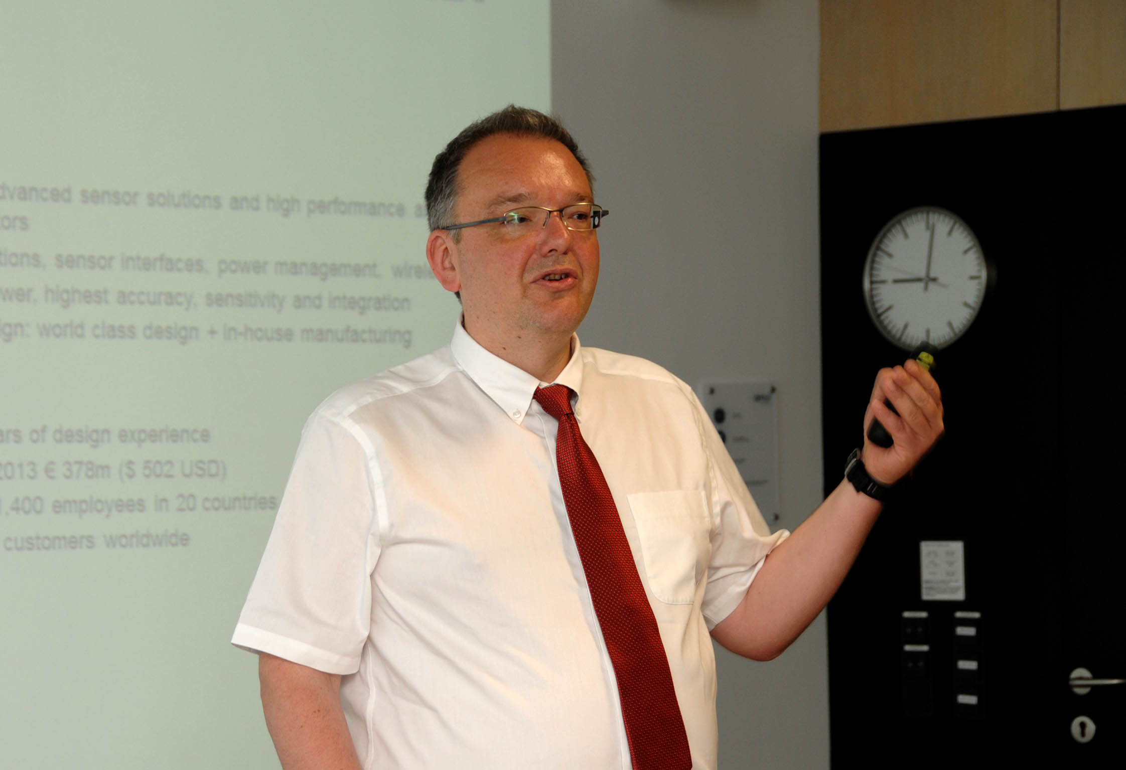
Thomas Riener, ams,executive vice president

NXP has sold its CMOS sensor business to Austrian mixed-signal chip firm ams.

NXP is currently in the middle of a merger with US chip firm Freescale Semiconductor.

Earlier this summer NXP also agreed to sell its RF power business to Chinese private equity firm Jianguang Asset Management  for $1.8bn.

The sale of the RF power business, which supplies RF power amplifiers to the mobile phone basestation market, seems to have been a element in the proposed merger of NXP with Freescale Semiconductor.

Proceeds from the sale of the RF Power business will be used to partly fund the acquisition of Freescale.

Now the sensor business, which includes humidity, pressure and temperature sensors, is to be sold to ams for an undisclosed amount.

According to Thomas Riener, executive vice president, marketing and strategy at ams:

“The acquisition of NXP’s CMOS sensor business expands our existing environmental sensor technologies and is a synergistic addition to our chemical sensor capabilities and smart lighting solutions. This portfolio makes ams the one-stop shop for environmental sensors.”

Ams is already has its sensors designed into smart phones and it is looking to expand this to wearables, smart buildings and medical markets.

It is looking to develop integrated sensor devices combing a processor, wired and wireless interfaces and power management.

“Environmental sensors can replicate and enhance human responses by monitoring and measuring smell, pressure and temperature. By capturing this information electronically, data-driven decisions can be made automatically and efficiently,” said Riener.

The new additions to the environmental sensor product portfolio are available for customer sampling now. Temperature and relative humidity sensor solutions will be in mass production early in 2016.

Richard Wilson

Comment: Can Germany keep Europe in the FD-SOI game?

German chancellor Angela Merkel on a visit to Infineon's Dresden fab

German chancellor Angela Merkel on a visit to Infineon’s Dresden fab

With FD-SOI now being proposed as the next generation semiconductor process technology, the epicentre for semiconductor manufacturing in Europe is shifting to Germany.

With the eclipse of both STMicroelectronics and NXP as major European manufacturers of chips, the new momentum for investment in wafer fabs seems to be coming from Germany alone.

That is if we class Imec in Belgium and France’s CEA-Leti as advanced semiconductor research facilities rather than commercial IC production wafer fabs.

In the past five years, Infineon has invested around €600m in its Dresden fab.

This month international chip foundry Globalfoundries extravagantly heralded the opening of “a new chapter in the Silicon Saxony story, building on almost 20 years of sustained investment in Europe’s largest semiconductor fab”.

The reason for this was a $250m investment in its fab in Dresden for development and initial production of its 22nm FD-SOI (full-depleted silicon-on-insulator) process technology platform called 22FDX.

This is significant because FD-SOI is now being proposed as the next generation semiconductor process technology which, like the finfet alternative being championed by Intel, is expected to drive chips to sub-10nm geometries.

Some observers believe that within five years volume digital chip production will be a square contest between finfet fabs and FD-SOI fabs.

Intel, Samsung and TSMC will be main protagonists with their wafer fabs in the US and Asia.

Globalfoundries is vying to be a prat of that fight. Its main fabs are in the US, courtesy of the IBM fab acquisition.

However, Globalfoundries alone of the big four chip manufacturers does not seem to have given up on Europe. As its continuing investment in FD-SOI capacity in Dresden demonstrates.

Globalfoundries has invested more than $5bn in the Dresden fab since 2009.

This would seem to make the European Commission’s grandiose but somehow directionless plans to create a European wafer fab irrelevant. NXP and ST do not seem than keen on the idea.

NXP is looking global with its acquisition of Freescale and ST has more pressing concerns at home.

So the EC’s only credible option seems to be to channel any chip investment it is prepared to make into the fabs in Dresden, Germany. This would seem unlikely.

So if Europe is to have the wherewithal to make sub-14nm FD-SOI chips in the future it looks like being in Germany, and largely thanks to the commitment of an international foundry, which unlike most other chips firms has not given up on making advanced chips in Europe.


Richard Wilson

ADI integrates 24-bit sigma-delta converters into sensor interface chip

ADI integrates 24-bit sigma-delta converters into sensor interface chip

ADI integrates 24-bit sigma-delta converters into sensor interface chip

Analog Devices has integrated 24-bit sigma-delta converters into analogue front end devices with up to eight differential inputs.

The AD7124-4 and AD7124-8 are integrated signal chain devices with a programmable gain amplifier, precision reference, reference buffers, current sources, temperature sensor and excitation sources all on-chip.

The AD7124-4 has four differential and seven pseudo-differential inputs and the AD7124-8 has eight differential and 15 pseudo-differential inputs.

The AFEs are designed to be used with devices with analogue outputs such as resistance temperature detectors, thermocouples, voltage/current inputs and current bridges.

The devices offer three user-selectable power modes. In the lowest power mode (255 µA) the converter delivers 21.7 noise free bits at low sampling rates.

The user-selectable power modes allow designers of programmable-logic controllers, process controllers, transmission systems and other industrial and instrumentation equipment to develop a single platform by precisely matching power/performance requirements for each use case.

Features

  • Three power modes
  • RMS noise
  • Up to 22 noise free bits in all power modes (gain = 1)
  • Output data rate
  • Rail-to-rail analog inputs for gains > 1
  • Simultaneous 50 Hz/60 Hz rejection at 25 SPS (single cycle settling)
  • Diagnostic functions (which aid safe integrity level (SIL) certification
  • Crosspoint multiplexed analog inputs
  • 4 differential/7 pseudo differential inputs
  • Programmable gain (1 to 128)
  • Band gap reference with 15 ppm/°C drift maximum (65 μA)
  • Matched programmable excitation currents
  • Internal clock oscillator

Analog Devices writes:

The AD7124-4 is a low power, low noise, completely integrated analog front end for high precision measurement applications. The device contains a low noise, 24-bit Σ-Δ analog-to-digital converter (ADC), and can be configured to have 4 differential inputs or 7 single-ended or pseudo differential inputs. The onchip low gain stage ensures that signals of small amplitude can be interfaced directly to the ADC.

One of the major advantages of the AD7124-4 is that it gives the user the flexibility to employ one of three integrated power modes. The current consumption, range of output data rates, and rms noise can be tailored with the power mode selected. The device also offers a multitude of filter options, ensuring that the user has the highest degree of flexibility.


Richard Wilson

Teachers get free Raspberry Pi skills in Google Digital Garage

Martin O’Hanlon will be leading teachers in Google Digital Garage

Martin O’Hanlon will be leading teachers in Google Digital Garage

Educating students of all ages in embedded design continues to be an important part of the activities of the Raspberry Pi Foundation.

Its programme of training teachers in embedded design based on Raspberry Pi is continuing apace with the numbers of Raspberry Pi-certified educators growing through its training events called Picademies.

It has set up five regional Picademies in the UK and with the support of Google a new Picademy in Birmingham.

Dubbed the Google Digital Garage, the Birmingham centre will be used by classroom teachers of any subject at primary, secondary or post-16 level.

The courses and workshops at the original Picademy in Leeds are run by renowned community member Les Pounder, who gives much of his time to helping adults and children create weird and wonderful projects.

At the Picademy@Google in Birmingham, Raspberry Pi community member and Minecraft wizard Martin O’Hanlon will be leading teachers in the the Raspberry Pi Foundation’s free CPD course.

The opening of the Google Digital Garage at the Library of Birmingham was attended by Eileen Naughton, MD of Google UK and Ireland, and Sajid Javid, Secretary of State for Business, Innovation and Skills.

All training events in Birmingham are free to attend and the following dates are available:

  • 27th – 28th August
  • 1st – 2nd October
  • 2nd – 3rd November
  • 7th – 8th December

Richard Wilson

Apple app developer taps into Microchip “supermarket”

Coderus Embedded software developer Coderus is raising its profile in the wireless IoT market by signing up to the Microchip Design Partner Program as an app developer specialist.

Suffolk-based Coderus sees Microchip as “a supermarket for core modules with which brands can build their products” and this will fit well with its custom software.

The software developer has worked with Microchip in a partnership agreement with Bowers & Wilkins, and has this has given it a software design capability to support the firm’s microcontrollers.

Coderus has developed a customisation toolkit for the Microchip range of microcontrollers.

Mark Thomas, managing director of Coderus, writes:

“We’ve designed the toolkit to give us a menu of choices so we can deliver a complete package that includes both embedded and mobile solutions, or we can choose one or several elements to work separately or to combine together.”

The firm also carries out functional and automated testing of the software apps before a product reaches the market.

Coderus has offices at Adastral Park, Ipswich and St John’s Innovation Centre, Cambridge. Company managing director Mark Thomas has attended Apple WWDC for the last 15 years and presently hold four patents from his work at BT Plc and is a co-Author on a published paper at Siemens.

In May, Coderus hosted a Google I/O extended event with keynote speeches streamed live from San Francisco to BT’s John Bray Lecture Theatre at Adastral Park.

Over 130 developers attended the event with live Google technology demo sessions.


Richard Wilson

TFT displays supplier offers Arduino shield for free

TFT displays supplier offers Arduino shield for free

TFT displays supplier offers Arduino shield for free

An Epson LCD controller shield board brings support for WQVGA and QVGA TFT displays to the Arduino Due development platform.

Independent distributor Ineltek UK is offering the Arduino shield free when you buy one of its selected TFT displays.

The S5U13781R01C100 TFT shield is based on the Epson S1D13781 controller IC with embedded 384kbyte display buffer which supports 8/16-bit direct and indirect CPU interfaces as well as SPI.

Resolutions supported range up to 480 x 272 at 24 bits per pixel and the device boasts hardware rotation of the display memory, Alpha Blending and Transparency and PIP Layer Flashing resulting in rich images even when used with low end processors.

The Arduino Due board is available online from Ineltek for around €35 and the TFT Shield Board is available for €15 or free when purchasing one of the supported displays.

Independent semiconductor distributor is offering the shield alongside a range of TFTs:

  • Tianma TM043NDH02 – WQVGA 4.3” 300 cdm-2 2.9mm thick module
  • Tianma TM043NBH02 – WQVGA 4.3” 280 cdm-2 4.15mm thick module
  • ImaginOrient IO04310006_v2 – WQVGA 4.3” 430 cdm-2
  • Hantronix HDA430-3GH-1 – WQVGA 4.3” 1000 cdm-2
  • Hantronix HDA351-LV –  QVGA 3.5”
  • Tianma TM035KDH03 – QVGA 3.5” 300 cdm-2


Richard Wilson

Southampton University holds electronics summer school

Southampton University holds electronics summer school

Southampton University holds electronics summer school

74 A-Level students from across the UK and beyond are taking part in the University of Southampton’s Electronics and Computer Science (ECS) annual summer school next week, with students coming from Dublin, Romania and Greece as well as the local area.

The summer school includes lectures covering varied aspects of ECS, from electronic and electrical engineering to computer science and software engineering.

Participants will be given the opportunity to tour the University of Southampton’s specialist facilities, such as the Tony Davies High Voltage Laboratory and the Southampton Nanofabrication Centre.

Sponsored by Imagination Technologies and JP Morgan, the summer school’s links with industry are intended to give participants an understanding of career options for graduates.

The course includes a day trip to sponsors so students can see how specialised electronics and computer science skills are applied and valued in business and industry.

Dr Geoff Merrett, Senior Admissions Tutor for ECS, says:

“We hope that by taking part in the summer school we have engaged the students in the subjects, inspired them to apply for a university place and opened their eyes to the exciting breadth of careers a degree in ECS can lead to”.

This year’s residential course, organised by Dr Geoff Merrett and Dr Reena Pau, is continuing the success of last year, with a series of talks from leading Southampton academics.


Richard Wilson

AMD SoC brings 4K graphics to Mini-ITX board

05aug15congatecCongatec has added low-power boards based on the Gen 2 AMD Embedded G-Series processor to its industrial-grade Mini-ITX motherboard range.

The SoC integrates an AMD Radeon graphics processor which means the board will support two independent displays and up to 4K (3840 x 2160 pixels) resolution.

These scalable motherboards offer TDP ranging between 5 and 15W max. 

The processor options include a 2.2GHz dual-core variant (10/15 W max. configurable TDP) or a 4x 1.2GHz quad-core platform (5/7 W max. configurable TDP) that is optimised for multiprocessing.

The 4K graphics support includes DirectX11.1 and OpenGL 4.2, and the two displays can be controlled via DisplayPort 1.2, DVI or LVDS.

Board expansion options include a PCIe x4 Gen 2.0 slot, 1x Mini PCIe, 2x USB 3.0, and 6x USB 2.0.


Richard Wilson

CUI power supply has 54V output for PoE

CUI power supply has 54V output for PoE

CUI power supply has 54V output for PoE

The latest 3000W front-end ac-dc CUI power supply is intended for power over Ethernet (PoE) applications.

The power supply is preset to output 54Vdc with a factory-adjustable output from 42V to 55V.

There is N+1 redundancy and hot swap blind-docking capability implemented through the use of a single connector that integrates ac, dc and I/O signals.

The PSE-3000-54 has a specified power density of 33.48W/cubic inch and is 94% efficient at 50% load.

It is a 1U unit measuring 40.64 x 101.6 x 355.6mm.

The main 54Vdc output delivers up to 55.5A with droop current sharing for paralleling of multiple units.

The output is floating and features isolation of 1500Vrms specifically for PoE applications.

For monitoring and control of the module, the PSE-3000-54 features system communications via I2C/PMBus protocol.


Richard Wilson

Cardiff gets new multi-million pound semiconductor centre

IQE_SiMachine1The UK is bidding to be a world-leading centre for research and production of compound semiconductors which are used in optoelectronics and power systems.

IQE, the semiconductor wafer foundry, is creating a joint venture with Cardiff University for the development and commercialisation of compound semiconductor technologies.

The JV will work closely with Cardiff University’s Institute of Compound Semiconductors (ICS), which in itself establishes world class CS research, development and innovation in Wales, with over £29m of funding from the Welsh and UK governments.

The ICS forms part of Cardiff University’s £300m investment in new research and innovation centres.

The venture is expected to attract other European partners to create a compound semiconductor cluster centred in Wales.

Dr Drew Nelson, chief executive of IQE, said:

“This JV with Cardiff University is a key step in creating the World’s first Compound Semiconductor Cluster, spanning basic research to full scale production. Our goal is to build this Cluster into one of Global significance and scale, leading to widespread economic benefits for the region.”

Compound Semiconductors have been identified in the European Commission’s “Horizon 2020” economic growth strategy, as a key technology enabler which is important for the re industrialisation of the EU.

The combination of the ICS with IQE’s existing wafer foundry in Cardiff establishes the core elements of a compound semiconductor ecosystem in Wales to bridge early stage research, product development, prototyping, and pilot production, through to high volume manufacturing.

Cardiff University recently announced the appointment of Professor Huffaker, a leading researcher from UCLA.

As part of the venture, IQE will contribute equipment with a market value of £12m, which will be matched by a £12m cash contribution from Cardiff University.

IQE will also license certain intellectual property (IP) to the JV.

Cardiff University Vice-Chancellor, Professor Colin Riordan, said:

“Coupling IQE’s infrastructure with Cardiff’s existing strengths in expanding areas of semiconductor devices and materials will create cutting-edge opportunities that will put us ahead of our competitors.”

Minister for Economy and Science, Edwina Hart said:

“Together with the appointment through our Sêr Cymru programme of Professor Diana Huffaker, a world renowned expert in the field, Cardiff is now well placed to become a hub for Compound Semiconductor research and exploitation.”

Richard Wilson