A stacked memory device which has the potential to achieve memory access speeds 14 times faster than today’s DDR4 has been demonstrated by eSilicon, Northwest Logic and SK Hynix.
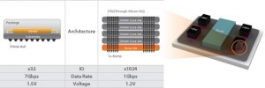
The stacked memory device is complaint with the JEDEC 2.5D packaging standard known as high bandwidth memory (HBM).
The chip uses an FPGA-based controller core and PHY for the HBM standard architecture implemented in a Hynix memory array.
eSilicon packaged the FPGA controller designed by Northwest Logic and HBM devices on an organic interposer.
First-generation HBM devices provide eight channels of 128-bit data running at one Gbit/s/pin for a total system throughput of 128Gbyte/s.
According to the companies, they say second-generation HBM devices double the throughput.
They claim this is approximately 14 times the throughput available from a DDR4 DIMM running at 2,600 Mbits/pin. HBM has both power and cost advantages over competing technologies.
Bill Isaacson, senior director, product marketing at eSilicon, writes:
“HBM and system-in-package technology hold great promise to break the power and performance bottlenecks designers are currently facing with regard to memory subsystems.
“This joint effort with Northwest Logic and SK Hynix validates that HBM is ready to enter mainstream use.”
The HBM Controller Core supports both Gen 2 (2 Gbit/s/pin) and Gen 1 (1 Gbit/s/pin).
Brian Daellenbach, president of Northwest Logic, expects to see increasing interest in HBM applications.

