Author Archives: david manners

Silicon Labs adds to capacitive sensing MCUs

Silicon Labs C8051F97x - block diagram

Silicon Labs C8051F97x – block diagram

Silicon Labs is sampling capacitive sensing microcontrollers (MCUs) for human-machine interfaces (HMI).

The C8051F97x MCU is for Internet of Things, home/building automation, consumer and industrial markets.

It targets battery-powered and capacitive touch sensing applications for handheld industrial devices, toys, gaming machines and remote controls, as well as touch-panel switch replacements for white goods such as washers, dryers, ovens and dishwashers.

The MCUs draw 200 µA/MHz active current, a two-microsecond wake time and a sleep mode energy consumption of 55 nA with brownout detector enabled and 280 nA sleep current with a 16.4 kHz internal oscillator.

They incorporate Silicon Labs’ SAR charge-timing capacitance-to-digital converter (CDC) technology which has 40 microsecond acquisition time.

Silicon Labs’ CDC technology offers superior noise immunity for reliable performance in challenging conditions and configurations such as thick laminate overlays, electrical noise or variances in printed circuit board (PCB) manufacturing.

This CDC hardware implementation is capable of measuring capacitance on a wide range of materials including PCBs, flex circuits, and indium tin oxide (ITO) on glass and film.

The F97x MCU family expands the capabilities of Silicon Labs’ C8051F99x low-power capacitive sensing MCUs with up to 43 capacitive sensing inputs, 32 kB flash memory, 8 kB RAM, seven DMA channels and a 16 x 16 multiply-accumulate (MAC) unit in QFN packages as small as 4 mm x 4 mm. The F97x MCUs integrate a 25 MHz pipelined 8051-compatible core, a precision oscillator, a 10-bit analog-to-digital converter (ADC), a temperature sensor, a voltage reference and four 16-bit general-purpose timer/counters.

Infineon expands Villach

Infineon - Peter Schiefer

Infineon Head of Operations – Peter Schiefer

Infineon is expanding its Austrian site in Villach in a project it calls “Pilot Space Industry 4.0”.

This, says Infineon, is an ‘ innovative concept for networked and knowledge-intensive production’.

Research on new materials and technologies will also be intensified.

Infineon’s expansion plans foresee investments and research costs amounting to a total of € 290 million, creating approximately 200 new jobs in the period from 2014 to 2017, primarily in R&D.

infineon’s Peter Schiefer, Says: “The continuing development of Villach is a part of our group-wide manufacturing strategy. At the site, important developments will be advanced and production-ready innovative technologies will be transferred by Infineon to other sites. At the same time our strategy will include expansion of our volume manufacturing on 300 millimeter thin wafers in Dresden and on 200 millimeter wafers in Kulim, Malaysia.”

Sabine Herlitschka, CEO of Infineon Austria, says: “With the expansion concept Villach is reinforcing its important role as a factory of innovation and a competence center for power electronics within the corporate group. We’re coupling the innovation factory in Villach with volume production in Dresden using the example of 300 millimeter thin wafer production for power semiconductors.”

Infineon will construct a complex for research, production and measurement technology workstations.

Logistics, miscellaneous infrastructures and the plant equipment will also be expanded to meet future demand. This will let Infineon mobilize the productivity and automation called for in international competition, while at the same time increasing flexibility.

Infineon has been actively engaged in the Industry 4.0 initiative from the very beginning; its pilot space in Villach is another step towards realising it.

A wide-scale research program with innovations in materials, processes, technologies and system expertise is the second pillar of the Villach site expansion, supporting development of the next generation of energy-efficient products.

Here the program focuses on the integration of innovative substrates such as gallium nitride and silicon carbide, on MEMS (Micro-Electro-Mechanical Systems) and sensor technologies as well as on the continuing development of 300 millimeter thin wafer technology.

Spansion adds to auto micros

Spansion Traveo automotive microcontroller S6J3100 series

Spansion Traveo automotive microcontroller S6J3100 series

Spansion is sampling its Traveo automotive microcontroller S6J3100 series with a CAN FD interface for in-vehicle networking.

The chip,is for various automotive applications including body control module (BCM), heating, ventilation and air conditioning (HVAC).

Bosch invented the CAN standard many years ago and since then worked to improve in-vehicle communication through innovative solutions. Bosch introduced CAN FD as a seamless upgrade of the classic CAN technology the first time at the International CAN Conference in 2012. Like classic CAN, CAN FD enables highly reliable vehicle control, taking advantage of higher data rates with only a small impact on current software and applications. Spansion has started to supply MCU products equipped with CAN FD.

As well as In the CAD FD interface operating at 5Mbps, the S6J3110 series comes with a maximum 4MB of flash memory and uses 55nm technology. It has Secure Hardware Extension (SHE) for network security and improved performance for connected cars, and partial wakeup for lowering power consumption.

The Spansion Traveo family of microcontrollers is based on the ARM Cortex-R5 core and tailored for a broad range of automotive applications.

In May 2014, Spansion introduced the first product of the family, the MB9D560 series for vehicle electrification utilised in hybrid electric vehicles (HEV) and electrical vehicles (EV).

TSMC full for the rest of the year

TSMC will run at 100% fab utilisation throughout the second half of the year, reports Digitimes.

Digitimes is quoting Morris Chang who also said that 20nm would account for 10% of total revenues in Q3 and 20% in Q4.

45nm and better processes account for half total revenues.

TSMC says it has 20 customers for its 16nm finfet process.

The company says it will set up a 300-400 person R&D lab to develop a 10nm process scheduled for trial production in 2015 and mass production in 2016.

Total capacity in 2013 was 15.67 million eight inch wafer equivalents. In 2012, it was 14.04 million.

AMS and Dialog in merger talks

AMS - DialogA new European semiconductor IDM could be on the cards if talks between AMS, the former Austria Micro Systems, and Dialog bear fruit.

Merger talks are underway between specialised foundry AMS and Dialog with AMS needing to make an offer for Dialog by July 24th if the acquisition is to happen.

AMS says: ‘AMS and Dialog confirm that the two companies are in preliminary discussions regarding a possible merger of equals of AMS and Dialog Semiconductor. These discussions are at a very preliminary stage and there can be no certainty that a transaction will be forthcoming.’

AMS had revenues of $502 million last year and has a market cap of $2.3 billion while Dialog had revenues of $903 million last year and has a market cap of $1.8 billion.


Technologists honoured in Queen’s Birthday List

Professor Thomas Walter Bannerman Kibble - Imperial

Professor Thomas Walter Bannerman Kibble – Imperial

The Queen’s Birthday Honours included knighthoods for Professor Thomas Walter Bannerman Kibble, CBE FRS Senior Research Fellow and Emeritus  Professor of Theoretical Physics at  Imperial College London, for services to Physics, and  Professor John Bernard Pethica, FRS FREng, Chief Scientific Adviser, National Physical Laboratory and Physical Secretary and Vice-President of The Royal Society for services to Science.

Dr Pamela Louise Makin, CEO BTG, becomes a Dame for the Life Sciences Industry.

The CBE goes to David James Gow, Inventor, I-Limb Hand, for services to Upper Limb Prosthetics.

The OBE goes to: Alexander David Beatty, Vice-President, Advanced Weapon Systems, Thales for services to the Aerospace and Defence Industries in  Northern Ireland; Dr Paul Martin Hawkins,  Managing Director and Chairman, Hawk-Eye  Innovations for services to Technology and Sport;  Dr Helen Elizabeth Mason,  Reader in Solar Physics, University of  Cambridge, for services to Higher  Education and to Women in Science, Engineering and Technology; Anupam Ojha,  Director, National Space Academy, for services to Science Education and Ms Belinda Parmar, CEO  Lady Geek for services to Women in Technology.

The MBE goes to: Dr Robert Samuel Andrews, Commercial Director, EW Simulation Technology,  for services to the Defence Industry; Professor William David Evans,  Consultant Physicist and Head of Medical Physics and Clinical Engineering, Cardiff and Vale University Health Board, for services to the NHS in Wales and Overseas, Mary Margaret, Grant Head of Science, Newry High School, for services to Education and to the community in Northern Ireland;  James Walker Kane Chairman, J W Kane Engineering,  for services to the Aerospace Industry in Northern Ireland; Professor Colin Robert McInnes, FREng FRSE Director, Advanced Space Concepts Laboratory, for services to Space Research, Science and Technology; Robert Joseph Schukai, Global Head, Mobile Technologies, Thomson Reuters for services to British trade and investment and to promoting STEM education.

Image: Imperial College - Professor Thomas Walter Bannerman Kibble

SPTS joins up with CEA-Leti on TSV

Crofton SPTS-Kevin-CroftonSPTS Technologies, the Newport etch, deposition and thermal processing specialist, has signed an agreement with CEA-Leti  to develop 3D-TSV technologies

The two-year agreement enters under the framework of the Nanoelec Research Technology Institute program which is led by CEA-Leti, and covers co-development of a range of deposition processes for next-generation 3D high aspect ratio through-silicon-via (TSV) solutions.

They  have already collaborated in the past, particularly on the development and optimization of an advanced MOCVD TiN barrier for high aspect ratio TSV.

To scale future 3D devices, new techniques will be needed to manufacture TSV’s of smaller diameter and higher aspect ratio than are used today.

Under this agreement, SPTS and CEA-Leti aim to develop production worthy solutions to address these challenges.

Previous collaboration has resulted in a number of key advancements in the formation of TSVs such as optimisation of an advanced metal organic chemical vapour deposition (MOCVD) TiN barrier for high aspect ratio TSV.

“ We plan to develop technology and processes that will further extend TSV aspect ratios beyond 20:1, with a particular focus on developing an MOCVD copper process as a seed layer to replace ionized PVD,” says SPTS CEO Kevin Crofton (pictured).

72 fabs closed in four years, says IC Insights

IC Insights Fab Closure72 fabs were closed between 2009-2013 and another nine fabs are to close this year, says IC Insights.

Since mid-2007, the IC industry has been paring down older capacity (i.e. 200mm and smaller wafers) in order to produce devices more cost-effectively on larger wafers.

A few fabs have been refurbished for production using larger wafers or for production of “non-IC” products.

One example is a 300mm wafer fab operated by Sony that closed, but was retrofitted and has returned to service manufacturing image sensors for the company.

40% of fab closures since 2009 have been 150mm fabs. Qimonda was the first company to close a 300mm wafer fab after it went out of business in early 2009. ProMOS and Powerchip closed their respective 300mm wafer fabs in 2013.

Regionally, semiconductor suppliers in Japan have closed 28 wafer fabs since 2009, more than any other country/region over the past five years. North America (23) and Europe (15) also had double-digit fab closures

Fabs closed or on the bubble in 2014 include Intel’s Fab 17 (200mm) in Hudson, MA; International Rectifier’s 150mm Fab 10 in Newport, South Wales; three fabs (two 150mm, one 125mm) at Renesas Electronics; two outdated NXP fabs (one 100mm, one 150mm) in Nijmegen, The Netherlands; and a 75mm wafer GaAs fab used by Panasonic Semiconductor to produce optoelectronic devices.

The closing of the two NXP fabs was announced a few years ago and was expected to be finalised in 2011, but was delayed due to strong demand for analog and logic ICs and some discrete components that are manufactured at these facilities. A 200mm fab continues to operate in Nijmegen.

As the cost of new wafer fabs and manufacturing equipment skyrockets, IC Insights expects several more companies to shutter older fabs and transition to a fab-lite or fabless business model in the coming years—good news that for foundries but bad news for equipment and material suppliers.

Spreadtrum overtakes Intel to be No.3 in baseband processors

Sravan Kundojjala

Sravan Kundojjala

Spreadtrum has overtaken Intel to grab the No.3 slot in the baseband processor market, says Strategy Analytics, which means that the second and third places in the baseband market are taken by a Taiwan company and a mainland China company.

MediaTek holds onto the No. 2 slot and Spreadtrum takes the No.3 slot pushing Intel down to No.4.

Qualcomm has a 66% share! MediaTek a 15% share and Spreadtrum a 5% share.

“For the first time in the last three years, Intel dropped out of the top-three baseband revenue share rankings as its 2G and 3G baseband shipments declined sharply in Q1 2014,” says SA analyst Sravan Kundojjala.

“Qualcomm grabbed two-thirds of the revenue share in the baseband market in Q1 2014, thanks to its diverse customer base and strong LTE product portfolio,” says SA’s Christopher Taylor, “Strategy Analytics calculates that Qualcomm’s LTE revenue share has now dropped to 91% in Q1 2014 from over 95% in Q1 2013. Qualcomm has a plenty of opportunities in terms of its LTE product-mix as less than 50 percent of baseband shipments were LTE basebands in Q1 2014.”

“MediaTek is now quickly establishing itself as a strong number two to Qualcomm in the baseband market,” says SA’s Stuart Robinson, “however, the company currently draws most of its growth from 2G and 3G markets only. In Q1 2014, MediaTek had no share in LTE basebands and we reiterate that the company needs to ramp up its LTE efforts with its upcoming LTE slim modems and applications processors to continue its growth trajectory.”


Bluetooth beacon draws under 20µA

EM Microelectronics Coin
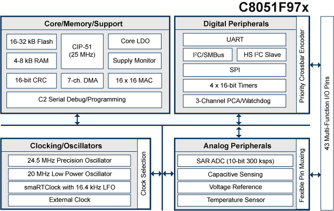
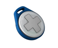
EM Microelectronic, the Swiss chip company, has introduced the COiN Bluetooth beacon. Which consumes less than 20µA average in a typical application, resulting in more than 18 months’ operation from a single CR2032 battery, which is included in the beacon.

COiN also contains a built-in pushbutton switch, guaranteeing that your beacons have a full charge when they are deployed. Integrated red and green LEDs provide users with feedback about the device’s operating mode.

The COiN’s integrated printed circuit antenna not only minimises cost, but maximises communication range. At the 0dBm output power setting, EM’s beacons can be detected 75 metres away by an iPhone 5S, and at maximum output power, that distance extends up to 120 metres.

Due to COiN’s optimised circuit architecture, it is completely immune to over-the-air attacks, meaning that a well-placed beacon is very secure. It cannot be “hacked” or modified unless the perpetrator has complete physical possession of the device.

COiN is shipped pre-programmed, complete with a Renata CR2032 battery and a weatherproof plastic enclosure, making it suitable for use at outdoor music festivals, sporting events and arenas, and anywhere a beacon is required to withstand the elements.

Though COiN is available in-stock pre-programmed and with a standard housing, the standard COiN hardware and firmware are easily modified to fit most applications. At the most basic level, COiN firmware can easily be modified to change the UUID, MAJOR ID, MINOR ID, output power, and beacon interval. These changes are useful for adapting the beacon for whatever smartphone software application/API is being used, segregating beacon populations and sub-populations, and for optimizing battery lifetime based on the desired use case.

Should more extensive firmware modifications be desired, EM offers a complete development kit. The COiN Development Kit includes five (5) COiN beacons, programming board and programming cable and is fully compatible with EM’s line of software development tools for the EM6819; EM’s ultra-low power microcontroller. Using these tools, customers have complete control over the firmware and can create their own Bluetooth Smart advertising packets and transmit real-time sensor data such as temperature, light level, battery voltage, or other physical phenomena.

The COiN enclosure can be customized to sport any embossed logo desired, making the beacon truly your product. No one will know that you leveraged EM’s decades-long experience and engineering effort and expertise to create your Bluetooth beacon, and we won’t say a word, though enclosure customizations are subject to a minimum purchase volume and tooling charges.

Not much larger than the CR2032 battery that powers it, COiN can be used almost anywhere. To assist in attaching and deploying COiN, EM offers a suite of accessories. The Key Fob Accessory snaps over COiN for attachment to key rings or for hook or loop-based attachment methods such as zip-ties. The Wall Mount Accessory can be nailed or screwed to a solid surface, and then COiN is snapped into place, completely hiding the Wall Mount. COiN can also be snapped into the Watch Band Accessory and any of a number of wrist bands for wrist-worn applications.

“COiN leverages EM’s expertise in ultra-low power wireless and computing as well as our high quality standards and synthesizes them into a high performance, Bluetooth beacon that is ready to deploy out of the box, but flexible enough to be modified for many different applications,” says EM president  Michel Willemin, “we are already engaged with many companies who are using COiN with their App, API, SDK, or service to improve their performance and lower their overall cost. We believe that the availability of such a flexible, optimised Bluetooth beacon will enable a truly pervasive Internet of Things.”