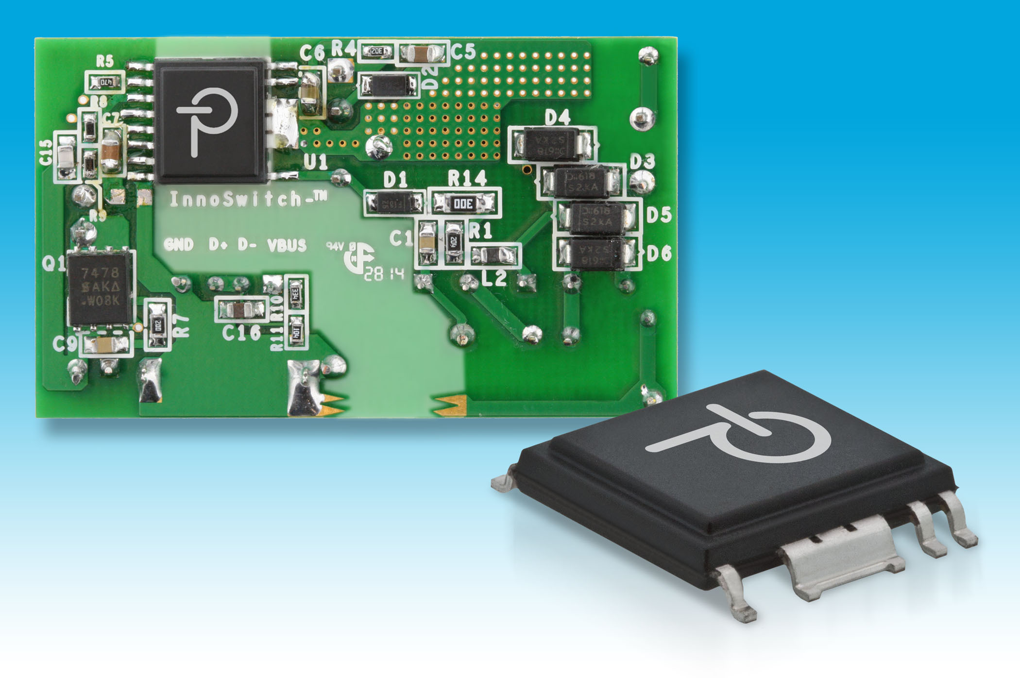
Author Archives: david manners

Power Integrations launches InnoSwitch

PI InnoSwitch

PI InnoSwitch

Today, Power Integrations announces  its InnoSwitch family of switcher ICs combines primary, secondary and feedback circuits into a single, worldwide safety-rated, surface-mount package.

“InnoSwitch ICs are the first switchers to combine the simplicity and low component count of primary-side regulation with the high performance of secondary-side control,” says Power Integrations vice-president Mike Matthews. “The InnoSwitch family’s high level of integration reduces power supply component count and its secondary-side regulated topology allows the use of simpler, lower cost, auto-wound transformers, yet improves production yield, resulting in significantly lower manufacturing cost. Two of the world’s leading mobile device makers are in production with chargers using InnoSwitch family ICs which incorporate FluxLink technology.”

InnoSwitch ICs will enable designers to exceed all global regulatory standards for efficiency and no-load consumption, claims the company, while minimising component count and providing accurate constant voltage and constant current up to 25W.

The InnoSwitch family is intended for use in smart mobile device chargers and adapters for a range of applications such as set-top boxes, networking equipment and computer peripherals.

Inside the device, secondary-side direct voltage and current measurements are communicated across the safety isolation barrier using high-speed digital FluxLink technology.

This proprietary feedback technique permits precise control without the need for a bulky optocoupler, Power Integrations says, without the performance compromises inherent in primary-side regulation (PSR), such as limited accuracy and efficiency and poor transient response versus no-load consumption.

InnoSwitch-based secondary-side regulated (SSR) designs are inherently less sensitive to the tolerance of external components such as transformers, diodes, resistors and capacitor,s the company says, which increases manufacturing yield and reduces total power supply cost.

Mobile device chargers up to  A can have a total component count as low as PSR designs, with accurate CV and CC control (±3% and ±5% respectively) and low voltage ripple.

InnoSwitch power-supply ICs include a high-voltage power mosfet, primary-side controller, FluxLink feedback technology and a secondary-side controller with synchronous rectification (SR). By combining the SR function with the secondary-side master controller and by leveraging the speed of the FluxLink communication channel, the SR switch timing is optimised for maximum efficiency.

The fast communication link also ensures reliable SR operation, eliminating shoot-through in either discontinuous conduction mode (DCM) or continuous conduction mode (CCM), even during transient loads and fault conditions. Effective SR operation in both DCM and CCM modes is especially beneficial in adaptive-voltage charger applications.

InnoSwitch ICs start up using bias current drawn from a high-voltage current source connected to the DRAIN pin, eliminating the need for external start-up components. An external bias winding reduces no-load and increases system efficiency during normal operation. The ICs also include comprehensive system-level features such as output over-voltage protection, overload power limiting, hysteretic thermal protection and frequency jitter to reduce EMI.

Samples are available now, priced at $0.59 to $0.78 in 10,000-piece quantities.

Reference design RDR-420 describes a 5V, 2A USB charger design and is available for download on the Power Integrations website.

david manners

Intel buys into Spreadtrum and RDA to push mobile x86 into China

Intel CEO Brian Krzanich

Intel CEO Brian Krzanich

Intel has bought a 20% share in the China state-owned company, Tsinghua Unigroup, which owns mobile chip developers Spreadtrum and RDA. The two chip companies will now make x86-based mobile ICs.

With China’s mobile IC specialist RockChip already co-developing chips with Intel, Intel has ensured that three of China’s major mobile chip-makers, which used to make ARM-based chips, will now make x86-based chips.

In December 2013, Unigroup bought Spreadtrum for $1.75 billion and in July this year Unigroup bought RDA for $907 million.

“This collaboration and investment will also enhance our ability to support a wider range of mobile customers in China and the rest of the world,” said an Intel spokesperson, “we will be able to deliver a broader portfolio of Intel architecture and communications technology solutions.”

“China is now the largest consumption market for smartphones and has the largest number of Internet users in the world,” said Brian Krzanich, Intel CEO, “these agreements with Tsinghua Unigroup underscore Intel’s 29-year-long history of investing in and working in China. This partnership will also enhance our ability to support a wider range of mobile customers in China and the rest of the world by more quickly delivering a broader portfolio of Intel architecture and communications technology solutions.”

Zhao Weiguo, chairman and president of Tsinghua Unigroup, says, “It has become a national priority of China to grow its semiconductor industry. The strategic collaboration between Tsinghua Unigroup and Intel ranges from design and development to marketing and equity investments, which demonstrate Intel’s confidence in the Chinese market and strong commitment to Chinese semiconductor industry, which will accelerate the technology development and further strengthen the competitiveness and market position of Chinese semiconductor companies.”

Spreadtrum will mske x86-based mobile SoCs coming on the market in H2 2015 to be sold both by Intel and Spreadtrum.

“The adoption of Intel’s architecture technology will enable us to accelerate the development of mobile SoCs that expand the breadth of our portfolio, benefiting handset makers addressing both China and the global market,” said Leo Li, chairman and CEO of Spreadtrum, in a statement. “We are pleased to embark on collaboration with Intel around these new product offerings.”

david manners

≤28nm processes account for 71% of all foundry revenues, says IC Insights

IC Insights - Foundry Revenue per logic waferTSMC has 84% of the total ≤28nm pure-play foundry market this year with $10.3bn in ≤28nm sales, says IC Insights.

Overall, ≤28nm foundry revenues will grow 72% in 2014.

Of the big four pure-play foundries (TSMC, GlobalFoundries, UMC, and SMIC), TSMC is the only one that is expected to have a higher revenue-per-wafer figure in 2014 than in 2010.

Of the big four foundries, TSMC is forecast to have the highest revenue per wafer in 2014 at $1,328, 27% higher than GlobalFoundries.

In contrast, UMC’s revenue per wafer in 2014 is expected to be only $770, 42% less than TSMC’s revenue per wafer.

Although the average revenue per wafer of the big four foundries is forecast to be $1,145 in 2014, the actual revenue per wafer is highly dependent upon feature size.

There is more than a 14-times difference between the 0.5µ 200mm revenue per wafer ($430) and the 28nm 300mm revenue per wafer ($5,850).

Even when normalising the figures by using the revenue per square inch, the difference is dramatic ($51.77 for the 28nm technology versus $8.56 for the 0.5µ technology).

Although TSMC has a very large percentage of its sales targeting ≤45nm production, its 2014 revenue per wafer is still forecast to be up only 14% when compared to 2009.

IC Insights believes that the entrance of GlobalFoundries and Samsung into the high-end foundry market over the past few years has put pressure on TSMC to keep its prices for leading-edge products competitive.

Although there will probably be only five foundries able to offer high-volume leading-edge foundry production over the next five years – TSMC, GlobalFoundries, UMC, Samsung, and Intel – these companies are likely to be fierce competitors and pricing will likely be under pressure as a result.

Before GlobalFoundries entered the foundry market, TSMC was by far the technology leader among the major pure-play foundries.

In 2014, 60% of TSMC’s revenue is expected to be from ≤45nm processing.  As expected, with GlobalFoundries’ fabs having a large portion of their capacity dedicated to producing AMD’s MPUs over the past few years, its processing technology is skewed toward leading-edge feature sizes.

In 2014, 57% of GlobalFoundries’ sales are forecast to be from ≤45nm production.

Although GlobalFoundries is expected to have a similar share of its sales dedicated to ≤45nm technology as TSMC in 2014, TSMC is forecast to have almost six times the dollar volume sales at ≤45nm as compared to GlobalFoundries this year ($14.8bn for TSMC and $2.5bn for GlobalFoundries).

In contrast, only 15% of SMIC’s 2014 sales are expected to come from devices having ≤45nm feature sizes, which is the primary reason why its revenue per wafer is so low as compared to TSMC and GlobalFoundries.

The vast majority of the increase in pure-play foundry sales in 2014 is forecast to be due to ≤28nm feature size device sales.

Although it is expected to represent 71% of total pure-play foundry sales in 2014, the >28nm pure-play IC foundry market is forecast to increase only 4% this year.

In contrast, the 2014 leading-edge ≤28nm pure-play foundry market is expected to be about $5.1bn, a 72% increase in size as compared to 2013.

Not only is the vast majority of pure-play foundry growth coming from leading-edge production, most of the profits that will be realized come from the finer feature sizes as well.

david manners

Qualcomm extends domination

Sravan Kundojjala

Sravan Kundojjala

Qualcomm’s baseband processor market share is at a record 68% with MediaTek No. 2 on 15%and Spreadtrum on 5% at No. 3, says Strategy Analytics.

The global cellular baseband processor market grew 17% year-on-year to reach $5.2 billion in Q2 2014.

Qualcomm, MediaTek, Spreadtrum, Marvell and Intel grabbed the top-five baseband revenue share spots in Q2 2014. Qualcomm continued its baseband market dominance with 68 % revenue share, followed by MediaTek with 15 % revenue share and Spreadtrum with 5 percent revenue share.

Sravan Kundojjala, Senior Analyst states, “Despite increased LTE baseband competition, Qualcomm managed to increase its baseband revenue share to an all-time-high of 68 % in Q2 2014. Qualcomm’s LTE Gobi slim modems and LTE Snapdragon applications processors all gained strong traction in Q2 2014 and featured in multiple flagship smartphones. Strategy Analytics calculates that LTE basebands accounted for over 45 % of Qualcomm’s total baseband shipments in Q2 2014. Strategy Analytics believes that still further LTE gains in the next few quarters provide further scope for market share gains.”

According to Stuart Robinson, Director of the Strategy Analytics Handset Component Technologies service, “In Q2 2014, MediaTek capitalised on its baseband-integrated applications processor momentum and solidified its number two position in the baseband market. Strategy Analytics estimates LTE basebands accounted for less than 1 percent of MediaTek’s total baseband shipments in Q2 2014. However, Strategy Analytics believes that MediaTek has the potential to emerge as the number two LTE baseband player in the second half of 2014, thanks to increased traction in China.”

Christopher Taylor, Director of the Strategy Analytics RF and Wireless Component service details, “Spreadtrum maintained its number three baseband revenue share position in Q2 2014, after overtaking Intel in Q1 2014. Strategy Analytics estimates that Spreadtrum’s W-CDMA baseband shipments registered 170 percent year-on-year growth in Q2 2014. Spreadtrum is well-positioned to grab W-CDMA market share dropped by Broadcom as it leaves the market.”

In the 2Q14 smartphone apps processor market, Qualcomm remains the company to beat in mobile processors with investments in CPU, GPU, DSP, RF, location and connectivity technologies well matched to current market trends

The chasing pack are now in a better position to compete as they are now shipping the key competitive products: namely LTE and baseband-integrated-Apps processors.

The global smartphone applications processor (AP) market grew 22 percent year-on-year growth to reach $5.2 billion in Q2 2014.

Based on Strategy Analytics estimates, Qualcomm, Apple, MediaTek, Spreadtrum and Samsung captured the top-five smartphone AP spots in Q2 2014. Qualcomm topped the smartphone AP market with 58 percent revenue share, followed by Apple with 14 percent revenue share and MediaTek with 13 percent revenue share.

According to Sravan Kundojjala, Senior Analyst, “Qualcomm continues to widen the lead and captured a record 58 percent revenue share in the smartphone AP market in Q2 2014, thanks to its strong momentum in LTE smartphones. Strategy Analytics believes that the multi price-tier Snapdragon processor portfolio continues to serve Qualcomm well.”

Stuart Robinson, Director of the Strategy Analytics Handset Component Technologies service details, “Strategy Analytics estimates that stand-alone AP unit share dropped to 21 percent in Q2 2014 compared to 28 percent in Q2 2013 and this can be attributed to increased shipments of low-to-mid range smartphones, which often feature baseband-integrated APs. Stand-alone AP vendors HiSilicon and Samsung are also now shipping baseband-integrated APs in volume to address mid-range smartphones.”

In the 2Q14 tablet apps market, Intel rose to the No.2 position in tablet APs

The non-Apple tablet AP market leadership position continues to change hands. Previously six companies have held the non-iPad tablet AP leadership position, which continues to be a challenging one to sustain due to the relative ease with which tablet OEMs can switch AP vendors.

The global tablet applications processor (AP) market registered a solid 23 percent year-on-year growth to reach $945 million in Q2 2014.

Apple, Intel, Qualcomm, MediaTek and Samsung captured the top-five tablet AP revenue share spots in Q2 2014. Apple maintained its tablet AP revenue share lead with 26 percent revenue share, followed by Intel with 19 percent revenue share and Qualcomm with 17 percent revenue share.

According to Sravan Kundojjala, Senior Analyst, “The non-Apple tablet AP market leadership position continues to change hands and during Q2 2014 it was Intel’s turn. Strategy Analytics notes that previously six companies held the non-iPad tablet AP leadership position, which continues to be a challenging one to sustain. Strategy Analytics believes that Intel is a on a good trajectory to achieve its 40 million tablet AP shipment goal in 2014.”

Stuart Robinson, Director of the Strategy Analytics Handset Component Technologies service adds, “During Q2 2014, HiSilicon, Marvell, MediaTek, NVIDIA and Qualcomm all registered significant shipment growth in the tablet AP market. Strategy Analytics believes that NVIDIA is well-positioned to grab high-profile tablet design-wins with its 64-bit Tegra K1 chip in the second half of 2014.”

david manners

Global Unichip expands interconnect IP

Global Unichip, TSMC’s design arm, has rolled out an expanded interconnect low power IP portfolio for ASICs targeting solid state drive (SSD) applications. The expansion covers ultra low power PCIe 3/4 PHY, DDR3/4, LPDDR3/4 CTRL/PHY and ONFi4.0 IO/PHY.

IP based on the 28HPM/HPC processes in the expanded portfolio are available now, while 16nm macros will be available in Q4 of this year. The first tape out targeting TSMC’S 16FF+ process is expected in October.

The company’s 16nm DDR4 PHY, taped out in November 2013, was the industry’s first.

The company is now expecting to tape out the industry’s first Application Processor platform IP to TSMC’s 16FF+ process at the start of 2015.

Among all NAND applications, SSD is the fastest growing with the Data Center and Enterprise segments showing the greatest potential. GUC addresses that with a complete low power IP portfolio for SSD controllers, including NAND I/O (ONFI, Toggle), DDR I/F (DDR3/4, LPDDR3/4) and Serdes I/F (PCIe-3/4, SATA3/SAS3).

“We have both a low power IP portfolio and an advanced technology roadmap to drive ASIC development for SSD markets to the next level of innovation,” says C. J. Liang, SVP of R&D at GUC.

GUC’s in-house IP portfolio includes DDR, high-speed networking interfaces, high -speed interface SerDes, data converters, hardened ARM cores, and multimedia IP. GUC’s IP ecosystem provides the flexibility to work with IP from GUC, TSMC and other vendors, creating the widest range of design options.

david manners

TSMC makes 16nm finfet ARM v8 processor for HiSilicon

TSMC President and Co-Chief Executive Officer Dr. Mark Liu

TSMC President and Co-Chief Executive Officer Dr. Mark Liu

TSMC says its collaboration with HiSilicon Technologies has produced the foundry segment’s first fully functional ARM-based networking processor with FinFET technology.

TSMC says its 16FinFET process has twice the gate density of TSMC’s 28HPM process, and operates more than 40% faster at the same total power, or reduces total power over 60% at the same speed.

“Our FinFET R&D goes back over a decade” says TSMC Co-CEO, Dr. Mark Liu.

TSMC’s 16FinFET has entered risk production with excellent yields, says the company, after completing reliability qualifications in November 2013.

Built on TSMC’s 16FinFET process, HiSilicon’s processor enables a significant leap in performance and power optimisation supporting high-end networking applications. By leveraging TSMC’s  heterogeneous CoWoS (Chip-on-Wafer-on-Substrate) 3D IC packaging process, HiSilicon integrates its 16-nanometer logic chips with a 28-nanometer I/O chip.

“This networking processor’s performance increases by three fold compared with its previous generation,” says HiSilicon President Teresa He, “it can support virtualisation, SDN and NFV applications for next-generation base stations,routers and other networking equipment.”


david manners

ARM sponsors Science Museum comms gallery

arm-scienceARM is sponsoring Information Age a new gallery to be opened at the Science Museum on 25 October.

Using interactive displays and experiences, the gallery will reveal personal stories about how life has been transformed by communication innovations over the last two centuries.

Information Age will be divided into six zones, each representing a different information and communication technology network; The Cable, The Telephone Exchange, Broadcast, The Constellation, The Cell and The Web.

The gallery will explore the important events which shaped the development of these networks, from the dramatic stories behind the growth of the worldwide telegraph network in the 19th century, to the influence of mobile phones on our lives today.

Re-live remarkable moments in history, told through the eyes of those who invented, operated or were affected by the new wave of technology, from the first BBC radio broadcast in 1922 to the dawn of digital TV.

Discover how wireless technology enabled lives to be saved and news of the Titanic disaster to be spread to the world within hours of the event, and hear the personal stories of the operators who worked on the Enfield Telephone Exchange, the last manual exchange which marked the end of an era in communication history.


david manners

Intel’s rectangular fin is “almost a miracle”, says Asenov

Intel’s 14nm process has done something which is “almost a miracle – extremely impressive,” says Professor Asen Asenov, Professor of Electrical Engineering at Glasgow University  and CEO of  statistical analysis specialist Gold Standard Simulations (GSS).

What impresses Asenov about what Intel has done with its 14nm process is Intel’s  fabrication of a rectangular fin.

“The fabrication is extremely good,” says Asenov, “I was initially disappointed by the Intel 22nm process but, seeing what they’ve done at 14nm, they’ve done a very good job on the fin.”

Two years ago Asenov was the first to point out t that the trapezoidal shape of the Intel 22nm FinFETs is suboptimal and results in stronger short channel effects and in up  to 15% reduction in current compared to an ‘ideal’ rectangular FinFETs.

“First, rectangular gives you better electrostatic control and better short channel effects – it gives stronger sensitivity to channel effect variations,” explains Asenov, “the  second thing is how much current can flow through the transistor. The current flow through the top of the transistor is not as  high, in a trapezoidal fin,  as you would want.”

“It would appear that Intel is a fast learner,” says Asenov. Intel has seen the force of  Asenov’s argument and gone for a rectangular fin at 14nm. “I think we may be able to claim some credit for that,” says Asenov.

As a result of the rectangular shape the drive current can, theoretically, be increased.

“It’s very difficult to increase the height of the fin and keep the rectangular shape,” says Asenov, “simultaneously they’ve increased the height of the fin and the reduction of the pitch gives a 1.7x improvement in the drive current.”

“But,” adds Asenov, “ in these small devices the drive current depends on the contact resistance . So the potential benefit is 1.7x but, if the contact resistance remains the same, the benefit will be small – it may drop to 1.2x or further.”

“The range of expectation could be very good – 1.5x to 1.7x,” adds Asenov, “or it could go back to the same performance as in the previous technology.”

The trouble is we don’t know.

“Intel hasn’t published too much data on the performance of these devices,” says Asenov.

There is another problem with the 14nm process – the SRAM doesn’t scale.

“With Intel’s finfet process, SRAM is very difficult to scale,” observes Asenov, “one of the most unattractive aspects of Intel’s 14nm is that they don’t have proper scaling of SRAM. With finfets the scaling of SRAM is difficult but ST is introducing 14nm SOI almost at the same time as 14nm finfet – and when FD-SOI is introduced at 14nm you can get back to the scaling of SRAM which reduces the cost of the chip.”

“14nm FD-SOI will be 40% cheaper than 14nm finfet,” reckons Asenov.

Asenov is clearly relishing the battle as different technologies fight for supremacy. “I’m glad we’re living in such a very dynamic time – it gives so many opportunities,” he says.

Two such opportunities  which have come the way of GSS recently are last November’s licensing of its statistical analysis tools to TSMC and last July’s licensing of tools to Globalfoundries.

On the GSS web-site a post looks at the situation in more detail.

First it cites a report on the achievement of the rectangular fin:

http://www.golem.de/news/intel-broadwell-lange-finfets-und-tiefer-gelegte-spulen-fuer-flache-tablets-1408-108494.html

asen1

Evolution of the Intel FinFETs from 22nm to 14 nm technology

From a first glance the reduced fin pitch and increased fin height suggest more than 1.7x improvement of the drive current. However the drive current will be strongly affected by the contact resistance and the extrinsic access resistance, both of which are expected to increase with the scaling of the pitch.

GSS has recently simulated very similar rectangular shape FinFETs and the results are published in [1]. The table below compares the geometry of the 14nm Intel FinFETs with the devices simulated in the above paper.

Intel 14nm FinFETs FinFETs in [1]
Fin Pich

42nm

40 nm

Fin Height

42nm

44 nm

Gate pitch

70nm

64nm

Based on the GSS predictive Ensemble Monte Carlo simulations in [1] illustrated below the ‘intrinsic’ pFinFET drive current of the transistors simulated in the paper can be more than 1.6 mA/mm; Vdd=0.75V. This is based on the assumption that 1.5 GP compressive strain can be introduced in the channel of the simulated transistors by suitable source/drain engineering. The velocity overshoot associated with the non-equilibrium velocity in the channel and the related high degree of ballisticity plays significant role in achieving such performance.

asen2

Strained Si pFinFET performance obtained form EMC, (b) Strain Si pFinFET carrier velocity. In the two graphs results of the EMC simulations are compared with results of ‘standard’ TCAD drift diffusion simulations before and after calibration.

However, the Ensemble Monte Carlo simulations do not include the contact and additional access resistances. If an access resistance of 1K ohm is included in the calibrated drift diffusion simulations the drive current drops from 1.6 mA/m to 1.2 mA/mm. Access resistance of 2K ohm can reduce the drive current to 1.0 mA/mm.

More details about the role of quantum effects, non-equilibrium transport, variability and reliability of the above FinFETs can be found in [1], which can be downloaded from the GSS web page at:

http://www.goldstandardsimulations.com/news/publications/


david manners

Plessey inks distie deal with Solid State Supplies

Plessey High Brightness LEDs - MAGIC

Plessey High Brightness LEDs – MAGIC

Plessey has entered into a distribution agreement with Solid State Supplies of Redditch to expand its European network with coverage in the UK and Ireland market for its GaN-on-Si LED products.

“Plessey’s GaN-on-Si technology looks set to cause major disruption in the LED lighting market,” says John Macmichael of SSS, “our in-house lighting division is already geared up to support lighting and luminaire designers with these new LEDs.”

“Plessey is very pleased to join forces with a distributor that has a focused lighting division already up and running, helping the significant number of lighting and luminaire makers in the UK,” says Plessey’s regional sales director David Owen, “Solid State Supplies has a strong portfolio of products to support the lighting eco system which is now enhanced by the addition of the Plessey GaN-on-Si LED product range. This will accelerate the time to market for Plessey LEDs in this region.”

Plessey’s MaGIC,(Manufactured on GaN-on-Si I/C) High Brightness LED (HBLED) technology has cut the cost of LED lighting by using standard silicon manufacturing techniques.

david manners

Glocal Unichip makes cost-effective, low-power server ASIC

GUC President Jim Lai

GUC President Jim Lai

Global Unichip, TSMC’s design arm, has made a remote management controller ASIC for server and desktop virtualization by adopting the first DDR3/4 PHY targeting TSMC’s 40LP process technology.

“The complexity of today’s server market is absolutely astounding. Performance was once king but today server SoC’s must also provide cost-effective performance. The innovation required to achieve this sweet spot, particularly at a 40nm manufacturing node requires real technical and business creativity and collaboration,” says GUC CEO Jim Lai.

GUC’s DDR 3/4 PHY is the first to be manufactured in 40nm process technology and provides low power, high performance and cost-effectiveness. GUC offers DDR3/4 PHY and controller production-proven turnkey solutions for all of TSMC’s most advanced process nodes including 40nm LP, 28nmHPM and 16nmFF+.

During the design and production process, engineers from both companies faced performance and time-to-market challenges. On the design side, the new device, the ASPEED’s AST2500 server SoC series and AST3200 Desktop Virtualization SoC had to achieve world- class performance on a cost-effective technology.

Key to success was designing to the performance sweet spot of GUC’s DDR3/4 high speed interface IP, a condensed package substrate, and a PCB through a precise DDR system simulation flow and measurement correlation.

The GUC IGADDRS03A DDR3/4 PHY high speed interface IP was implemented with a multiple oxide memory I/O design that capitalized on the combo DDR3 and DDR4 low power and high speed operation. The IP supports user-friendly PHY self training that shortens first system boot up time and reduces engineering resources. The IGADDRS03A integrates with both third party and GUC’s DDR3/DDR4 memory controllers.

“GUC brought in-depth IP, process technology and packaging know-how to the challenge of providing cost-efficient performance to a 40nm SoC. Collaboration was key to leveraging these skills across our two companies’ engineering team,” says ASPEED Technology CEO Chris Lin.

david manners