Author Archives: david manners

MTC1 1W DC/DC converters with wide input range from Murata

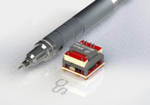
Murata MTC1 1W DCDC

Murata MTC1 1W DCDC

Murata has launched the MTC1 series of 1W regulated single output DC/DC converters with nominal input voltages of 12 or 24 VDC and accommodate a 2:1 input range around the selected nominal which allows for use in designs with different nominal input voltages or in situations where wide voltage deviations might occur.

It is aimed at applications such as medical, industrial, telecommunications, battery powered systems, and process automation.

The range comprises six single output models providing 3.3, 5 or 12 VDC for both the 12 and 24 VDC nominal inputs. No additional regulation components are required since the MTC1 output is fully regulated to within +/- 0.5% of stated output.

A voltage trim pin allows adjustment of the output voltage by +/- 10% to suit any special voltage requirements. A remote on/off pin provides the ability to disable the output for application power saving.

Input to output isolation conforms to the international safety insulation standard UL60950 (Pending). With its certification to the medical safety standard ANSI/AAMI ES60601-1 for 2 MOOPs the converter is suitable for use in a wide range of medical and healthcare applications. The MTC1 can operate up to 105 degrees C with derating.

“The MTC1 with its 34% smaller footprint, UL60950 reinforced insulation and 3rd edition medical safety standard compliance offers enhanced product features in a miniature package,” said Ann-Marie Bayliss, product marketing manager at Murata Power Solutions.

Features

  • UL 60950 recognition pending for reinforced insulation
  • ANSI/AAMI ES60601-1, 2 MOOPs recognition pending
  • 3kVAC isolation test voltage ‘Hi Pot Test’
  • Continuous short circuit protection
  • Output Voltage Trim
  • Remote on/off pin
  • No electrolytic capacitors
  • Operating temperature range -40°C to 100°C
  • 2:1 Input Range

You can view the full datasheet »


david manners

Infineon, NXP develop NewP@ss next-gen ID chip

Infineon, NXP and chip card security specialists Giesecke & Devrient (G&D) have developed technology for e-passports and ID cards which, as well as storing a users’s biometric data, can also record visa data and arrival and departure stamps.

Shutterstock- passports

NewP@ss is e-passport technology

Called “NewP@ss”, the research project cost €30m, half of which was covered by business and industry partners and the other half by the governments of five member states of the European Union. The German share was about €8.7m.

NewP@ss makes it possible to update ePassports and similar documents during their period of validity rather than replacing them, for example if a name is changed due to marriage or an address changed.

The secure use of digital identity documents for smartphones and tablets was also researched during the development of the chip.

The experts considered open architectures and tested new security mechanisms at both software and hardware levels. The primary focus was placed on contactless communication with an eID Card, secure mobile user authentication and confidential data input and output within a protected computing environment.

Biometric travel documents are currently issued in all 28 EU states with its approximately 500 million residents. Electronic identity cards are used in 23 European countries.

Other European states have already announced that they will introduce electronic identity cards in the next few years or begin issuing the next generation, which this research project helped to develop.

A total of 120 states have distributed around 500 million electronic travel documents since 2006.

david manners

Melexis evaluation kit supports ToF sensors

Melexis is supporting its time-of-flight (ToF) sensing technology with the EVK75023 evaluation kit which accompanies its MLX75023 QVGA (320x240pixels) resolution ToF sensors.

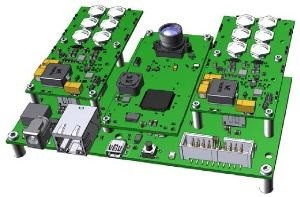
Melexis EVK75023 for ToF sensors

Melexis EVK75023 for ToF sensors

This new hardware platform enables implementation of more advanced human machine interfaces (HMIs).

Co-developed with BlueTechnix, the EVK75023 is a 130x105x60mm board for assessment of ToF sensing capabilities under challenging conditions, where the detrimental influence of ambient light variations must be addressed. Thanks to the constituent MLX75023 imaging device, it can deal with up to 120klux of background light.

The EVK75023 has a high bandwidth Gigabit Ethernet interface, through which real-time 3D images are output at frame rates of up to 60fps, according to Melexis. These can be used to recognise complex gestures. Via a C-based API or via the Matlab SDK, users can easily develop their own communication interfaces.

The platform consists four main elements:

  •  A pair of illuminating units – each with a set of six LEDs capable of producing a peak optical output of 10W
  • A sensor board – incorporating the MLX75023 sensor, a standard M12 lens mount plus objective with a field of view up to 60°, a quad-channel data converter and programmable logic (through which both the sensor and the LEDs are controlled)
  • An ARM-based processing board – featuring an i.MX6x Freescale microprocessor, which is responsible for compiling the acquired ToF data then subsequently communicating this to a laptop, via the Gigabit Ethernet connection, for analysis
  • An interface board – on to which all of these different subsystems are placed.

“By using Melexis’ automotive-grade ToF offering, automobile engineering teams will be able to deploy HMIs which are robust enough to deal with difficult working environments, where they are exposed to dramatic alterations in light levels, while still hitting the necessary price-points to ensure economic viability,” says Melexis’ Kristof Lieben. “This evaluation kit gives engineers the functionality needed to make an initial appraisal of the design set up, so that it can be optimised for the particular surroundings.”

david manners

GloFo completes acquisition of IBM microelectronics

GlobalFoundaries completes its acquisition of IBM microelectronics

GlobalFoundaries completes its acquisition of IBM microelectronics

GlobalFoundaries (GloFo) has completed its acquisition of the IBM microelectronics business.

“We have significantly enhanced our technology development capabilities and reinforce our long-term commitment to investing in R&D for technology leadership,” says GloFo CEO Sanjay Jha.

“We have added world-class technologists and differentiated technologies, such as RF and Asic, to meet our customers’ needs.”

GloFo says the deal ‘solidifies its path to advanced process technologies at 10nm, 7nm, and beyond’.

In RF, GloFo now has world-class capabilities in both RF silicon-on-insulator (RFSOI) and SiGe technologies, which are complementary to its existing mainstream technology offerings. The company says it will continue to invest to deliver the next generation of its RFSOI roadmap and looks to capture opportunities in the automotive and home markets.

In Asics, GLoFo says it now has technology leadership in wired communications. This enables it to provide the design capabilities and IP necessary to develop high-performance customised products. The company plans to increased investments to develop additional Aic products in storage, printers and networking. The most recent Asic family, announced in January and built on GloFo’s 14nm-LPP technology, has been well accepted in the marketplace.

Global Foundries CEO Sanjay Jha

Global Foundries CEO Sanjay Jha

GloFo increases its manufacturing scale with fabs in East Fishkill, NY and Essex Junction, VT.

The transaction builds on significant investments in the burgeoning Northeast Technology Corridor, which includes GloFo’s Fab 8 in Saratoga County, NY and joint R&D activities at SUNY Polytechnic Institute’s College of Nanoscale Science and Engineering in Albany, NY. The company’s presence in the northeast US now exceeds 8,000 direct employees.

The acquisition includes an exclusive commitment to supply IBM with some of the world’s most advanced semiconductor processors for the next 10 years. GloFo also gets direct access to IBM’s continued investment in world-class semiconductor research, solidifying its path to advanced process geometries at 10nm and beyond.

david manners

Silego adds reverse-current blocking

Silego, the programmable mixed signal specialist, has added reverse-current blocking to its dual-channel, self-contained integrated power-switch product line.

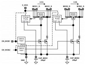
Silego SLG59M1603V block diagram - reverse-current blocking

Silego SLG59M1603V block diagram – reverse-current blocking

Adding reverse-current blocking makes the SLG59M1603V suitable for low-voltage power-rail distribution, power-rail sequencing, or any other two-power-rail application where power flow from load to source cannot be allowed, said the company.

The SLG59M1603V operates from 2.5V to 5V and, because of its proprietary and patented CuFET technology, is designed to handle continuous load currents up to 4.5A per channel in a small footprint TDFN package.

With internal charge pumps, output discharge circuitry, and separate On/Off controls, both channels of the SLG59M1603V are completely independent. As a result, each can be configured for different power-rail applications without affecting the operation of the other.

Also, by virtue of the CuFET technology, both channels can be combined in parallel for higher-current applications up to the total power dissipation of the package or up to 8.5A, whichever is lower.

Available in a space-saving 14-pin 1.0 x 3.0 mm STDFN package, the SLG59M1603V is fully specified from -40°C to 85°C.
Key SLG59M1603 specifications include:

Ultra-low RDSON: 16mΩ per channel
Continuous load current: Up to 4.5A per channel
Vdd supply voltage range: 2.5V to 5.5V
Wide power-rail voltage range: 1V to Vdd
Low reverse-current leakage when off: 0.5µA
Adjustable in-rush current/Vout slew rate control via external capacitor
Over-temperature protection
Low operating supply current: 50µA
Low-supply current when off: 1µA
Fast, internal discharge

david manners

Oregon researchers fabricate silver

Chih-hung Chang, a professor in the Oregon State Uiniversity College of Engineerin

Chih-hung Chang, professor in the Oregon State Uiniversity College of Engineering

Engineers at Oregon State University report that they have invented a way to fabricate silver, opening broad applications in microelectronics, sensors, energy devices, low emissivity coatings and even transparent displays.

A patent has been applied for on the technology, which is now available for further commercial development.

“There’s a great deal of interest in printed electronics, because they’re fast, cheap, can be done in small volumes and changed easily,” said Chih-hung Chang, a professor in the OSU College of Engineering, “but the heat needed for most applications of silver nanoparticles has limited their use.”

OSU scientists have solved that problem by using a microreactor to create silver nanoparticles at room temperatures without any protective coating, and then immediately printing them on to almost any substrate with a continuous flow process.

“Because we could now use different substrates such as plastics, glass or even paper, these electronics could be flexible, very inexpensive and stable,” Chang said. “This could be quite important and allow us to use silver in many more types of electronic applications.”

Uses could include solar cells, printed circuit boards, low-emissivity coatings, or transparent electronics. A microchannel applicator used in the system will allow the creation of smaller, more complex electronics features.

The research was supported by the National Science Foundation and Oregon Built Environment and Sustainable Technologies Center.

david manners

Nordic integrates Bluetooth Smart and NFC Touch-to-Pair

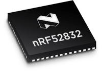
Nordic Semiconductor SoCNordic Semiconductor has put Bluetooth Smart and NFC for Touch-to-Pair on its nRF52832 SoC which has a 64MHz ARM Cortex-M4F processor, a 2.4GHz multi-protocol radio, and automatic power optimisation.

According to Nordic Semi, with a 215 CoreMark the nRF52832 delivers up to 60% more generic processing power than competing products and, thanks to its ARM Cortex-M4F, up to an additional 10 times the floating point and twice the DSP performance. And at 90 CoreMark/mA the SoC is up to twice as power efficient as competing solutions, the company claims.

Read Electronics Weekly Bluetooth Smart news »

The SoC also includes on-chip peripherals for glueless interfacing to external components such as sensors, displays, touch controllers, LEDs, keypads, motors, digital microphones, and audio Codecs, making it suitable for wearables, remote controllers, toys, smart home devices and appliances, and wireless charging.

Development Kits, QFN samples, software and documentation are available. Volume production is scheduled for December 2015.

Specification

  • Single chip 2.4 GHz multi-protocol SoC
  • 32-bit ARM Cortex-M4F Processor
  • 1.7v to 3.6v operation
  • 512kB flash + 64kB RAM
  • Supports concurrent Bluetooth Smart/ANT protocol operation
  • On-chip NFC tag for Out-of-Band (OOB) pairing
  • Up to +4dBm output power
  • -96dBm sensitivity, Bluetooth Smart
  • Thread safe and run-time protected
  • Event driven API
  • On air compatible with nRF24L and nRF24AP series
  • 2 data rates (2Mbps/1Mbps)
  • PPI – maximum flexibility for power-efficient applications and code simplification
  • Automated power management system with automatic power management of each peripheral
  • Configurable I/O mapping for analog and digital I/O
  • 3 x Master/Slave SPI
  • 2 x Two-wire interface (I²C)
  • UART (RTS/CTS)
  • 3 x PWM
  • AES HW encryption
  • Real Time Counter (RTC)
  • Digital microphone interface (PDM)
  • On-chip balun

See alsoFuture is Smart, IoT is Bluetooth

david manners

ITF2015: The business model for IoT

The Imec Technology Forum in Brussels this week addressed the question: What is the business model for IoT?

Internet of Things - IoT

Internet of Things – IoT

“People are looking for new business models for IoT,” said Harmke de Groot, Imec’s senior director perceptive systems for the IoT. “It is important to develop these – McKinsey says that the biggest problem with IoT is that business models need to be developed.

“We are developing this together with our partners,” de Groot added. “There will be many new business models.”

The thing about IoT is that everyone knows how to connect machines to each other, and everyone has been connecting things to other things for many years. Connecting things together is easy, but making money out of connecting things together is difficult.

“At Imec, IoT is not just about connecting devices,” said de Groot, “we concentrate on intuitive devices. In that respect we focus on IoT connected to cloud computers.”

The aim is to develop “intuitive and autonomous” systems, said de Groot.

david manners

Bidding war for ISSI ends in China victory

ISSI-bids-ChinaAfter six competing bids, it looks as though ISSI is going to the Chinese. Although Cypress has upped its bid to $22.6 a share, this is below the $23 offer from Chinese private equity consortium Uphill Investments, led by Summitview Capital of Hong Kong.

It is believed that the China government wants ISSI to form the basis of a national DRAM industry.

Here is Cypress CEO T J Rodgers’ latest letter to the ISSI board, which looks like a withdrawal from the contest:

June 24, 2015

Jimmy S M Lee
Executive Chairman

Scott D. Howarth
President and Chief Executive Officer

Integrated Silicon Solution, Inc.
1623 Buckeye Drive
Milpitas, California 95035

Messrs. Lee and Howarth,

On behalf of Cypress Semiconductor Corporation (“Cypress”), I hereby submit our best and final offer for Integrated Silicon Solution, Inc. (“ISSI”) and attach a revised draft Agreement and Plan of Merger between ISSI and Cypress (the “Revised Definitive Merger Agreement”).  Cypress is increasing its offer to acquire ISSI to a price of $22.60 per share (the “Revised Offer”), while maintaining its previously outlined ticking fee of $0.10 per share per quarter beginning October 1, 2015.  Our strategic and financial analysis indicates this is the maximum price justified for ISSI in order for the deal to create long-term value for our shareholders.  Again, we are prepared to put the Revised Definitive Merger Agreement reflecting our Revised Offer, signed by me to demonstrate our sincerity and strong commitment to closing this transaction, into escrow through our lawyers today.  We strongly believe that our Revised Offer clearly represents a superior, risk-adjusted proposal to the transaction contemplated by the current Agreement and Plan of Merger (the “Uphill Agreement”) with Uphill Investment Co. (“Uphill”).

Cypress’s Revised Offer demonstrates committed financing, eliminates regulatory risk by agreeing to possible ISSI SRAM divestitures, and includes a ticking fee to compensate for any unforeseen delay in closing.  Additionally, we continue to believe that a transaction with Cypress would benefit not only ISSI shareholders, but also ISSI customers due to the increased breadth and strategic capabilities of the product offerings of the combined companies.  Conversely, the Uphill transaction continues to be burdened with risks and uncertainties with respect to the:

Continued existence of a contractual financing out clause for the lender supporting the Uphill transaction,
Continued complexities of the government-mandated Taiwan divestitures, and
A potential prolonged investigation by The Committee on Foreign Investment in the United States (“CFIUS”)—the inter-agency committee of the United States Government responsible for reviewing the national security implications of foreign investments in U.S. companies.
As we have noted previously, had we been included in your sale process, your shareholders would have reaped two significant benefits: a more time-efficient price-discovery process and the capture of a potential incremental $0.56 per share per quarter, which was instead misspent on an unnecessary breakup fee.  To the extent the ISSI board decides to proceed with the Uphill transaction, and that higher risk transaction faces significant delays or fails to close, Cypress may be interested in acquiring ISSI in the future, but expects that our offer at that time may be substantially below this Revised Offer.  Finally, we fully expect that Uphill, with its backing from the Chinese government, will increase its offer price subsequent to the release of this letter, thereby acknowledging and attempting to compensate for the higher level of risk in completing their transaction.

Sincerely,

T.J. Rodgers
President and Chief Executive Officer

david manners

ITF2015: Affordable scaling is the key, says ASML

Affordable scaling is the key to the semiconductor industry, it was said at the Imec Technology Forum in Brussels.

ASML CEO Peter Wennink large“If we are not getting scaling affordable there are trillions at stake,” ASML CEO Peter Wennink told the forum, adding that he is an accountant not a technologist so he understands about costs.

Affordable scaling depends on getting EUV (extreme ultraviolet lithography) into the manufacturing process at the 7nm node and on a successful
mix-and-match approach with immersion, said Wennink.

Double patterning will get the industry to 10nm but then it needs either multi-patterning or techniques like directed self assembly, Imec’s process senior vice-president An Steegen told the forum.

“At 10nm multi- patterning means exploding complexity, ” said Wennink.

EUV solves that problem, but it is not there yet. The light source which ASML uses from its San Diego subsidiary Cymer is currently 80W, and ASML has demonstrated 110W, but some people are saying 350W is needed.

Wennink said two years of “solid progress” had debunked scepticism about the viability of getting a sufficiently powerful light source.

Up-time for EUV steppers needs improving, he said. Currently it averages 55% and one customer has achieved 86% during one week. Wennink said ASML’s target is to reach 86% average by the end of 2015.

david manners