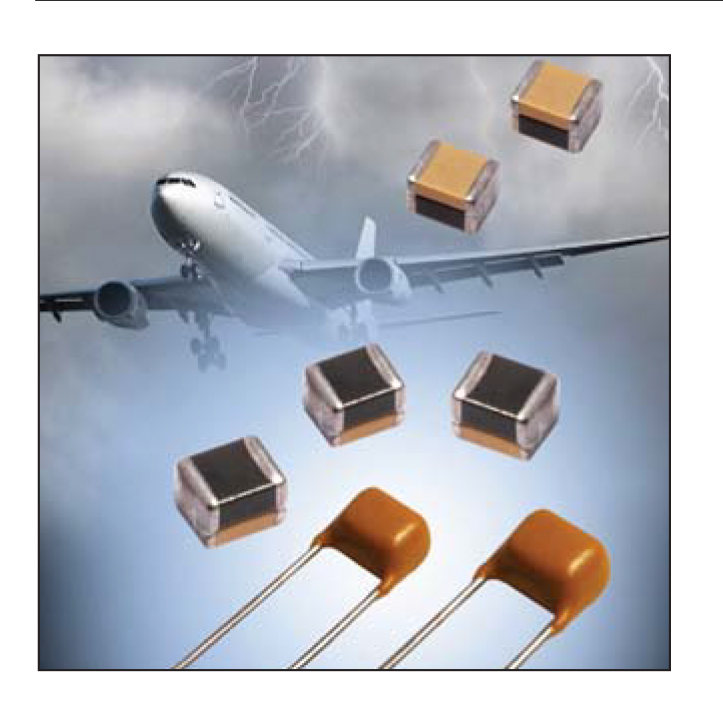
Author Archives: david manners

AVX launches CapGuard automotive varistor/capacitor

AVX CapGuard

AVX CapGuard

AVX has introduced the radial leaded CapGuard automotive series of combined multilayer varistor (MLV) and high capacitance, temperature stable X7R multilayer ceramic capacitor (MLCC) technology in a single, hi-rel device.

The CapGuard Series exhibits bi-directional transient voltage protection, excellent EMI/RFI attenuation over a wide frequency spectrum, and multi-strike capabilities in a compact, radial configuration with a conformal epoxy coating that provides enhanced resistance against harsh environments, mechanical shock, and vibration.

Qualified to AEC-Q200, the devices exhibit exceptional current and energy handling capabilities, and are suited to protect sensitive electronics from high voltage transients, as well as to filter out high frequency EMI/RFI noise generated by switch mode power supplies, motors on DC lines, I/O lines in electronic circuits, inductive switching, relays, and other applications.

“Our new radial leaded CapGuard Automotive Series devices allow design engineers to protect sensitive components against high voltage transients, and filter out unwanted EMI/RFI noise from the circuit, with a single, dual function component,” says AVX’s Jiri Machanicek, “built for durability in harsh environments, CapGuard Series devices are the ideal choice for applications that require EMI filtering, surge protection, high reliability performance, enhanced mechanical resistance, and the conservation of board space.”

The CapGuard Automotive Series is currently available with two working voltages (26VDC and 45VDC), two capacitances (0.47µF and 1µF), both with ±20% tolerance, and two energy ratings (0.6J and 0.7J).

Rated for operating temperatures spanning -55°C to +125°C, and ESD-rated to 25kV (HBM ESD Level 6), the RoHS compliant series is available in two sizes: 20 and 21, both of which measure, at a maximum, 5.99mm wide, 7.49mm high, and 4.5mm thick, and have a lead diameter of 0.508mm. Lead spacing for size 20 parts with straight leads is 2.54mm, and lead spacing for size 21 parts with kinked leads is 5.08mm.

CapGuard Automotive Series devices can be shipped in bulk or on one of two standard tape and reel packaging options. Lead time for the series is 27 weeks.

david manners

Imec offers silicon photonics prototyping

Imec offers silicon photonics prototyping

Imec offers silicon photonics prototyping

Imec and its partners have completed a three-year programme to make a number of silicon photonics technologies accessible for industry and academia.

Within the ‘ESSenTIAL’ programme (Essential) funded by the EC, Imec has worked with CEA-Leti (France), Tyndall Institute (Ireland), VTT (Finland), IHP (Germany), TNO (the Netherlands) and CMC (Canada), to develop advanced multi-project-wafer services as well as packaging services for silicon photonics.

The services were made accessible to industrial players  – both small- and medium-sized companies – enabling them to test silicon photonics.

Silicon photonics is a key enabling technology for a wide range of markets, from optical interconnect networks in data centers to disposable biosensor chips for immunoassays. In essence, silicon photonics builds on the technology portfolio and economy of scale of CMOS fabs to manufacture sophisticated photonic integrated circuits with a combination of passive devices – in particular wavelength and polarisation selective devices – and active devices such as optical modulators and detectors.

The Essential program has expanded the services of ePIXfab, an alliance of European entities set up in 2006 to support the emergence of a fabless silicon photonics ecosystem. ePIXfab has provided affordable multi-project wafer (MPW) services to fabless R&D teams that are developing photonic circuits. European users received some benefits based on EU funding, but the ePIXfab services were provided globally.

Within the Essential project high speed active devices (up to 25Gbit/s) were added to the MPW offering. ePIXfab has also started to organise extra MPW runs on two silicon photonics technology platforms with unique features, at IHP and at VTT.

In total over 200 silicon photonics circuit designs were prototyped at imec, Leti, IHP or VTT, including close to 50 designs from companies.

Another major achievement of the project was the creation of silicon photonics packaging services at Tyndall Institute.

Given the shortage of skilled engineers in silicon photonics, especially at the design level, Essential has spent considerable resources on training activities. Over 110 experts were trained in regular six-monthly training events and several hundreds more were reached through webinars. And Essential has conducted 80 feasibility studies with European SMEs, which resulted in at least 22 new projects and over 30 project proposals.

During Essential the MPW operation for silicon photonics has been integrated into Europractice IC service, marking a milestone for the further growth of Europe’s silicon photonics.


david manners

Q2 PC shipments fall 11.8%

PC-shutterstock_148831151

Q2 PC shipments fall 11.8%

Year-on-year PC shipments fell 11.8% in Q2, to 66.8 million units, says IDC, after a 6.7% decline in Q1.

Gartner puts the decline at 9.5% to 68.4 million.

For the full year IDC sees a 4.4% decline and Gartner a low-to-mid single-digit decline.

Lenovo is number one supplier with a 20.3% share, followed by HP with 19.4%, Dell with 14.5%, Acer 6.6% and Asus 6.5%.

Apple’s 5.1 million computer shipments would earn it the number four slot with a 7.8% share which translates into a 15% revenue share.

“Although the second quarter decline in PC shipments was significant, and slightly more than expected, the overall trend fits with expectations,” said Loren Loverde, Vice President, Worldwide PC Trackers & Forecasting.

“We continue to expect low to mid-single digit declines in volume during the second half of the year with volume stabilizing in future years. We’re expecting the Windows 10 launch to go relatively well, though many users will opt for a free OS upgrade rather than buying a new PC. Competition from 2-in-1 devices and phones remains an issue, but the economic environment has had a larger impact lately, and that should stabilize or improve going forward.”

“The U.S. market was in line with forecasts, declining -3.3% from a year ago, after avoiding the global market declines over the past five quarters. Soft retail demand, short term weakness from inventory reductions, some cannibalization from competing devices, and low demand for large commercial refreshes are among the factors that reduced PC shipments,” said Rajani Singh, Senior Research Analyst, Personal Computers.

“Nevertheless, moving forward, we expect a healthy second half as inventory and purchase decisions pick up following the launch of Windows 10. Emerging product categories will remain a bright spot as attention shifts to convertibles and Chromebooks in the commercial as well as consumer segments.”

david manners

Black arsenic phosphorus could replace silicon

Crystals of semiconducting black arsenic phosphorus Image: Andreas Battenberg / TUM

Crystals of semiconducting black arsenic phosphorus
Image: Andreas Battenberg / TUM

Layered semiconducting black arsenic phosphorus could be an alternative to silicon, say researchers at the Technical University of Munich (TUM).

TUM chemists have developed a semiconducting material in which individual phosphorus atoms are replaced by arsenic. In a collaborative international effort, American colleagues have built the first field-effect transistors from the new material.

Black arsenic forms extremely thin layers. The array of possible applications ranges from transistors and sensors to mechanically flexible semiconductor devices. Unlike graphene, whose electronic properties are similar to those of metals, black arsenic phosphorus behaves like a semiconductor.

A co-operation between the TUM, the University of Regensburg, the University of Southern California (USC) and Yale has produced a field effect transistors (fet) made of black arsenic phosphorus.

The compounds were synthesised by Marianne Koepf at the laboratory of the research group for Synthesis and Characterization of Innovative Materials (SCIM) at the TUM.

The fet  were built and characterized by a group headed by professor Zhou and Dr Liu at the Department of Electrical Engineering at USC.

The new technology developed at TUM allows the synthesis of black arsenic phosphorus without high pressure, which requires less energy and is cheaper. The gap between valence and conduction bands can be precisely tuned by adjusting the arsenic concentration.

“This allows us to produce materials with previously unattainable electronic and optical properties in an energy window that was hitherto inaccessible,” says professor Tom Nilges, head of the research group for SCIM.

With an arsenic concentration of 83% the material exhibits an extremely small band gap of only 0.15 electron volts, making it predestined for sensors which can detect long wavelength infrared radiation. Lidar (light detection and ranging) sensors operate in this wavelength range, for example. They are used, among other things, as distance sensors in cars. Another application is the measurement of dust particles and trace gases in environmental monitoring.

A further interesting aspect of these new, two-dimensional semiconductors is their anisotropic electronic and optical behavior. The material exhibits different characteristics along the x- and y-axes in the same plane. To produce graphene-like films the material can be peeled off in ultra thin layers. The thinnest films obtained so far are only two atomic layers thick.

The work was supported by the Office of Naval Research (ONR), the Air Force Office of Scientific Research (AFOSR), the Center of Excellence for Nanotechnologies (CEGN) of King Abdul-Aziz City for Science and Technology (KACST), the German Research Council (DFG) and the TUM Graduate School.

david manners

ADI launches quad-channel protector

22jul15ADI-ADG5462F_pcAnalog Devices (ADI) has introduced a quad-channel protector and two multiplexers offering ±55V overvoltage protection (OVP) for precision converters, amplifiers and other components that operate from a voltage of 4.5V up to 36V.

According to ADI the ADG5462F quad channel protector, ADG5248F 8:1 multiplexer and ADG5249F differential 4:1 multiplexer offer ±55V OVP in power-on and power-off stages and protect against hot-swapping and operator miss-use events, protecting downstream analogue components.

By providing on-chip fault diagnostics, the devices detect and avoid defective channels, which simplifies fault detection algorithms and improves system uptime, said the company.

The chips help users to define fault-trigger levels independent of primary supplies, and by removing the need for multiple discrete protection components, ADI claims they optimise PCB area and simplify the design process. The devices are optimised for precision instrumentation, process control and avionics applications.

The ADG5248F 8:1 multiplexer and ADG5249F differential 4:1 multiplexer maximise throughput for small signal measurement such as thermocouples or resistance temperature detectors (RTDs) by offering low-fault leakage of 70nA and on-leakage of 20nA. These levels ensure that the user can take accurate measurements when other multiplexer I/O channels are in an over-voltage fault condition.

Key Features:

  • Over-voltage detection on source pins
  • Minimum secondary supply level: 4.5V single-supply
  • Over-voltage protection up to ±55 V
  • 4kV HBM (human body model) ESD (ADG5462F)
  • VSS to VDD analog signal range
  • ±5V to ±22V dual-supply operation
  • 8V to 44V single-supply operation
  • Fully specified at ±15V, ±20V, +12V, and +36V
  • Operating Temperature Range −40°C to +125°C

ADG5462F: Ultra-low on-resistance of 10ohm and on-resistance flatness of 0.5ohm minimises system total harmonic distortion and enhances noise performance.

ADG5248F/49F: Ultra-low charge injection of 0.8pC and on-capacitance of 19pF enables higher accuracy, faster channel switching in multiplexed systems

david manners

Chrystek’s voltage controlled oscillator

Crystek voltage controlled oscillator - cvco55fl

Crystek voltage controlled oscillator – cvco55fl

Crystek’s CVCO55FL-0271-0310 voltage controlled oscillator (VCO) operates from 271 MHz to 310 MHz with a control voltage range of 0.5V~4.5V.

The company reports that its latest VCO features a typical phase noise of -114dBc/Hz @ 10KHz offset and has “excellent” linearity. Output power is typically +0dBm.

The device is available in the industry-standard 0.5×0.5-inch SMD package. Input voltage is 5V (typical), with a maximum current consumption of 5mA.

Pulling and pushing are minimised to 2.0MHz and 1.0MHz/V, respectively. Second harmonic suppression is -15dBc (typical).

The CVCO55FL-0271-0310 is suitable for use in applications such as digital radio equipment, fixed wireless access, satellite communications systems, and basestations.

david manners

Cree buys APEI

Dr Alex Lostetter - president and CEO of APEI

Dr Alex Lostetter – president and CEO of APEI

Cree has bought APEI, the power modules and power electronics specialist, to extend its power and RF business and accelerate the market for SiC power modules.

The companies already collaborate on multiple government contracts.

“Extending our research and development capabilities with APEI, a leader in wide bandgap power R&D, will help us accelerate delivery of a full spectrum of SiC power modules,” says Cree’s Frank Plastina, executive VP of Cree Power and RF.

“Joining forces with the market leader in silicon-carbide power gives us an opportunity to commercialize our products faster,” said Dr. Alex Lostetter, president and CEO of APEI. “This ideal combination of chip technology and packaging will give us first-mover advantage, helping us to set the industry standard for power modules.”

The APEI team, now Cree Fayetteville, Inc., will continue to be based in Fayetteville, AR., and will operate as part of Cree’s Power and RF business. Under the terms of the agreement, Cree will acquire APEI in a merger transaction.

Under the terms of the agreement, Cree will acquire APEI in a merger transaction. The transaction is not targeted to have a material impact on Cree’s fiscal 2016 earnings.

More Electronics Weekly stories on Cree »

david manners

Gadge Panesar joins UltraSoC

Gadge Panesar - UltraSoC CTO

Gadge Panesar – UltraSoC CTO

UltraSoC, the embedded systems debug specialist, has appointed Gajinder (“Gadge”) Panesar as its CTO, succeeding UltraSoC co-founder Dr Andrew Hopkins.

Panesar joins UltraSoC from Nvidia. Before Nvidia he was Chief Architect at Picochip and Mindspeed and has worked at ST, Inmos and Acorn. He holds 20 patents.

“Gadge is one of the foremost SoC architects in Europe, combining profound technical knowledge, strong commercial nous and a distinctive leadership style,” says Rupert Baines, UltraSoC CEO, “Gadge will take UltraSoC forward, drawing upon his extensive experience of complex SoCs, tool flow development and managing hardware/software interactions: we’re very fortunate to have been able to recruit him.”

“In an increasingly connected world, UltraSoC’s ability to diagnose and solve problems remotely becomes extremely powerful,” says Panesar.

UltraSoC’s s products de-risk the SoC design process, accelerate time-to-market, improve quality and reduce costs, by empowering pre- and post-silicon debug, and enabling hardware/software co-design, co-integration and unified debugging. UltraSoC’s technology can be used to monitor and refine the features and performance of an SoC – even after the device has been designed into an end product and is working in the field.

“UltraSoC’s core silicon IP and software technology has been created, licensed and proven in silicon,” says Hopkins, “it is ready to enable a broad range of analytic applications, giving the company a unique, differentiated offering. I’ve now decided it’s time to move on. I’m glad to be ‘passing the baton’ to someone with Gadge’s experience, energy and system know-how and am confident that he will lead the engineering team with the integrity and passion UltraSoC is known for.”

david manners