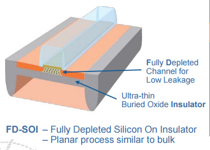
Global Foundries 22FDX diagram
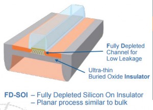
Globalfoundries has launched a 22nm FD-SOI process called 22FDX which claims to deliver ‘finfet-like performance and energy-efficiency at a cost comparable to 28nm planar technologies’.
Target markets are IoT, mainstream mobile, RF connectivity and networking.
While some applications require the ultimate performance of finfet transistors, most wireless devices need a better balance of performance, power consumption and cost and 22FDX provides, says GloFo, the best path for cost-sensitive applications by leveraging the industry’s first 22nm two-dimensional, FD-SOI technology.
It offers the industry’s lowest operating voltage at 0.4V, enabling ultra-low dynamic power consumption, less thermal impact, and smaller end-product form-factors. The 22FDX platform delivers a 20% smaller die size and 10% fewer masks than 28nm, as well as nearly 50% fewer immersion lithography layers than foundry finfet.
“The 22FDX platform enables our customers to deliver differentiated products with the best balance of power, performance and cost,” says GloFo CEO Sanjay Jha, “in an industry first, 22FDX provides real-time system software control of transistor characteristics: the system designer can dynamically balance power, performance, and leakage. Additionally, for RF and analogue integration, the platform delivers best scaling combined with highest energy efficiency.”
22FDX leverages the high-volume 28nm platform in GloFo’s 300mm production line in Dresden with an investment of $250 million for technology development and initial 22FDX capacity.
This brings the company’s total investment in Fab 1 to more than $5 billion since 2009. The company plans to make further investments to support additional customer demand. GloFo is partnering with R&D and industry leaders to grow a robust ecosystem and to enable faster time-to-market as well as a comprehensive roadmap for its 22FDX offering.
GloFo’s 22FDX platform enables software-control of transistor characteristics to achieve real time tradeoff between static power, dynamic power and performance. This platform consists of a family of differentiated products architected to support the needs of various applications:
• 22FD-ulp: For the mainstream and low-cost smartphone market, the base ultra-low power offering provides an alternative to FinFET. Through the use of body-biasing, 22FD-ulp delivers greater than 70 percent power reduction compared to 0.9 volt 28nm HKMG, as well as performance equivalent to FinFET. For certain IoT and consumer applications, the platform can operate at 0.4 volt, delivering up to 90% power reduction compared to 28nm HKMG.
• 22FD-uhp: For networking applications with analog integration, this offering is optimized to achieve the same ultra-high performance capabilities of FinFET while minimizing energy consumption. 22FD-uhp customizations include forward body-bias, application optimized metal stacks, and support for 0.95V overdrive.
• 22FD-ull: The ultra-low leakage offering for wearables and IoT delivers the same capabilities of 22FD-ulp, while reducing leakage to as low as 1pa/um. This combination of low active power, ultra-low leakage, and flexible body-biasing can enable a new class of battery-operated wearable devices with an order of magnitude power reduction.
• 22FD-rfa: The radio frequency analog offering delivers 50 percent lower power at reduced system cost to meet the stringent requirements of high-volume RF applications such as LTE-A cellular transceivers, high order MIMO WiFi combo chips, and millimeter wave radar. The RF active device back-gate feature can reduce or eliminate complex compensation circuits in the primary RF signal path, allowing RF designers to extract more of the intrinsic device Ft performance.
GloFo has been working with key customers and ecosystem partners to enable optimised design methodology and a full suite of foundational and complex IP. Design starter kits and early versions of process design kits (PDKs) are available now with risk production starting in the second half of 2016.
david manners
 Hot on the heels of the acquisition of ISSI by a Chinese private equity company, another China-based fund has bid for Micron valuing it at $23 billion. The offer of $21 a share is 19% over its pre-bid closing price.