Author Archives: david manners

Antenova adds Sinica for 1559MHz-1609MHz satellite bands

05aug15antenovaAntenova, the Hatfield antenna specialist, has launched an embedded GNSS antenna, named ‘Sinica’, which operates on the 1559MHz–1609MHz satellite bands.

Sinica is suitable for all positioning applications on the 1559MHz-1609MHz bands, the company says. It operates with all of the public satellite constellations – GPS, GLONASS, Baidou and Gallileo – which means it can provide accurate positioning combined with global coverage.

The Sinica antenna is created from FR4 materials and new dielectric constant laminate substrates. According to the company it uses a new approach to antenna design, which has enabled the company to create an antenna with the high performance of a ceramic patch antenna, in a low profile part that can be placed neatly within a small printed circuit board.

Sinica is designed for devices that need accurate positioning or tracking globally, which means it is suitable to use in drones, network devices and wearable electronics, or any other portable device or tracking application.

Antenova’s product designers recently introduced the concept of ‘design for integration’ (DFI), which considers how the antenna will operate when it is embedded with a manufacturer’s product. Antenova’s antennas are used within a customer’s design, so they are designed to provide RF performance from within the device, and to make the integration of the RF elements easier for the designer.

The antennas are supplied on tape-and-reel.

david manners

IQE joins Obama initiative

drewnelson

Drew Nelson

obama

President Obama and Vice President Biden

IQE has been announced as a key partner in a new consortium to establish the United States’ first Integrated Photonics Institute for Manufacturing Innovation (IP-IMI).

Created as part of President Obama’s National Network for Manufacturing Innovation (NNMI), the IP-IMI was launched this week in Rochester, NY by US Vice President Biden as the sixth of nine new manufacturing institutes designed to bring industry together with academia and government to advance the state-of-the-art in the design, manufacture, testing, assembly, and packaging of photonic integrated circuits and establish US Leadership in Integrated Photonics.

“IQE is proud to have been named as one of 55 key industrial partners in this important project led by SUNY to accelerate photonic capabilities and manufacturing in the U.S,” says IQE CEO Dr Drew Nelson, “the importance of the rapidly growing photonics technology industry cannot be overestimated and is already having a major impact in areas such as communications, energy efficiency, healthcare and safety and security systems. Inclusion as a key partner in this new US Manufacturing Institute is testament to IQE’s reputation as a global world leader in compound semiconductor materials, a key enabling technology (KET) for photonics.”

The consortium comprises 55 leading industrial partners, including Intel, IBM, Infinera, HP, Honeywell, Rockwell, Seagate and TI along with numerous other leading edge companies, universities and laboratories, and is led by the Research Foundation of the State University of New York (SUNY). IQE’s role in the consortium is to provide advanced epitaxy services to the Institute partners.

The IP-IMI has been awarded federal funding of $110 million by the Department of Defense, which is expected to yield total public-private investment of more than $610 million which will enable the institute to focus on developing an end-to-end integrated photonics ecosystem in the U.S., including domestic foundry access, integrated design tools, automated packaging, assembly and test, and workforce development. The Institute will develop and demonstrate innovative manufacturing technologies for:

  • Ultra-high-speed transmission of signals for the internet and telecommunications
  • New high-performance information-processing systems and computing
  • Compact sensor applications enabling dramatic medical advances in diagnostics and treatment
  • Multi-sensor applications including urban navigation, free space optical communications and quantum information sciences
  • Other diverse military applications including electronic warfare, analog RF sensing, communications, and chemical/biological detection
  • All of these developments will require cross-cutting disciplines of design, manufacturing, packaging, reliability and testing.
  • Photonics is widely recognised globally as a key enabling technology that has significant potential to revolutionize a wide range of commercial, industrial and defense applications, including:
  • Revolutionizing communications
  • Creating dramatic energy savings at high-performing data centres
  • Dramatically improving medical technologies
  • Improving safety and security operations

The institute will provide central facilities through which academia, SMEs and large corporations can access latest technology for design and manufacture of photonics devices providing a route to commercialisation through high-value, high-volume manufacturing.

More IQE stories on Electronics Weekly »

david manners

Infineon on-track to 34% y-o-y growth

Infineon had calendar Q2 revenue of € 1,586 million – up 7% on calendar Q1 – for a profit of €245 million at a margin of 15.4%. Infineon expects a 1% revenue increase in calendar Q3 and a 34% increase for the full year.

Dr Reinhard Ploss, Infineon

Dr Reinhard Ploss, Infineon

“Revenue, earnings and margin rose significantly in the quarter, despite an increasingly difficult business environment,” says Infineon CEO Reinhard Ploss, “for the full fiscal year, we therefore continue to forecast revenue and a Segment Result Margin within the ranges previously predicted. The integration of International Rectifier is progressing according to plan.”

Between its four main operating units, revenues split: Automotive €621 million, Industrial Power Management €269 million, Power Management and Multimarket €517 million and ChipCard and Security €172 million.

Overall group operating income improved from €79 million in calendar Q1 to €119 million in calendar Q2 while net income for calendar Q2 came in at €109 million, well ahead of the previous quarter’s €65 million.

Payment of the purchase price for International Rectifier had given rise to a negative Free Cash Flow of €1,880 million in calendar Q1.

Net cash provided by operating activities from continuing operations rose from €135 million to €432 million. The gross cash position went up from €1,656 million on March 31, 2015 to €1,842 million at the end of calendar Q2.

The net cash position improved over the same period from a negative amount of €176 million to stand at a positive amount of €49 million at June 30, 2015.
With these figures, Infineon is now back within the target range for its three capital management objectives, namely gross cash of between 30 and 40% of revenue, a positive net cash position, and a moderate level of debt.

All four operating segments will contribute to revenue growth in 2015.

Investments during the 2015 fiscal year are expected to be in the region of €800 million. This figure includes investments in plant and equipment at existing factories and in intangible assets including capitalized development costs.

Specifically included in these investments are €60 to €70 million for readying the second shell in Kulim, Malaysia, for volume production and €21 million for the purchase of Qimonda patents in conjunction with the settlement reached with the insolvency administrator of Qimonda AG.

Depreciation and amortization will increase to around €750 million, mostly as a result of acquisition-related charges.

Read more Infineon stories on Electronics Weekly »


david manners

Toshiba licenses ARM Cortex-A53

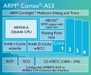
ARM Cortex A53 chip diagram

ARM Cortex A53, based on ARMv8-A

Toshiba has licensed the ARM Cortex-A53 processor, the most power-efficient ARMv8-A processor capable of seamlessly supporting 32-bit and 64-bit code.

Toshiba will deploy the processor to develop ASSPs such as ApP LiteT application processors that offer well balanced power-efficiency and performance with 64-bit capability, and custom products such as FFSA (Fit Fast Structured Array) and ASIC for industrial, networking, IoT, automotive and data storage products.

The Company expects to bring products to market at an early date, it says.

The industrial market is seeing strong demand for 64-bit capabilities and high reliability. The network market requires high-speed, low-power-consumption operation, real time processing and multi-clustered storage systems for huge data handling and data encryption. IoT products require power-efficient microprocessors, and applications relying on enormous storage capacity need an expanded memory address space. Toshiba will develop products to meet these various demands.

According to the company, the processor will allow Toshiba to hasten the development of highly featured, high performance systems that meet the functional safety requirements of ISO26262 for the automotive market and to provide customers with solutions for next generation automotive applications.

The Cortex-A53 processor features an 8-stage in-order pipeline, and strengthened data access / instruction fetch techniques. It also features ARM NEON technology with enhanced multimedia handling capabilities in addition to 128-bit SIMD ordering capabilities, as well as a cryptographic engine that accelerates encryption handling such as AES (Advanced Encryption Standard) and SHA (Secure Hash Algorithm) by extending architectures.

“Toshiba’s commitment to build SoCs based on Cortex-A53 further highlights the diverse range of use cases for the industry’s leading low-power 64-bit processor,” said Nandan Nayampally, vice president, marketing, CPU group, ARM. “The Cortex-A53 will deliver new levels of compute performance into power and space constrained environments in automotive, IoT and networking infrastructure applications and the processor safety package enables Toshiba to create products compliant with the latest functional safety standards.”


david manners

QuickLogic introduces multi-core EOS sensor hub

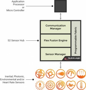
EOS - QuickLogic Flexible Fusion Engine S2-Sensor Hub Block-Diagram

EOS – QuickLogic Flexible Fusion Engine S2-Sensor Hub Block-Diagram

QuickLogic has introduced a triple core sensor hub called EOS.

The justification for sensor hubs is that: “It is power-prohibitive to do sensor processing on the host processor,” according to QuickLogic vice-president Brian Faith.

The three cores are: an ARM Cortex M4F MCU, a front-end sensor manager and a QuickLogic proprietary core which it calls Flexible Fusion Engine (FFE). A fourth core could be integrated into the hub’s FPGA fabric.

The FFE and and sensor manager handle the bulk of the algorithm processing, which minimises the duty cycle for the floating point MCU.

This approach lowers aggregate power consumption, and enables mobile, wearable and IoT device designers to introduce next generation sensor-driven applications, such as pedestrian dead reckoning (PDR), indoor navigation, motion compensated heart rate monitoring, and other advanced biological applications within their power budgets.

The EOS platform includes a hardened subsystem specifically designed for always-listening voice applications.

With its dedicated PDM-to-PCM conversion block, and Sensory’s Low Power Sound Detector (LPSD) technology, the EOS system enables always-on voice triggering and recognition while consuming less than 350 microAmps.

“It solves the problem of doing voice recognition at low power,” says Faith.

EOS has 2,800 effective logic cells of in-system reprogrammable logic that can be used for an additional FFE or customer-specific hardware differentiated features.

The EOS S3 platform and QuickLogic’s SenseMe library are compliant with Android Lollipop (5.0+) as well as various RTOSes.

Since the platform is sensor and algorithm agnostic, it can support third party and customer-developed algorithms through QuickLogic’s industry-standard Eclipse Integrated Development Environment (IDE) plugin.

The IDE provides optimised and proven code generation tools as well as a feature-rich debugging environment to ensure quick porting of existing code into both the FFE and the ARM M4F MCU of the EOS S3 platform.

Applications include:

  • Always-on, always-listening voice recognition and triggering
  • Pedometry, pedestrian dead reckoning, and indoor navigation
  • Sports and activity monitoring
  • Biological and environmental sensor applications
  • Sensor fusion including gestures and context awareness
  • Augmented reality
  • Gaming

Processor Cores

  • 180DMIPS of aggregate processing capability
  • 578KB of aggregate SRAM for code and data storage

QuickLogic Proprietary microDSP Flexible Fusion Engine

  • 50KB SRAM for Code
  • 16KB SRAM for Data
  • Very long instruction word (VLIW) microDSP architecture
  • 50µW/MHz
  • As low as 12.5µW/DMIPS

ARM Cortex M4F

  • Up to 80MHz
  • Up to 512KB SRAM
  • 32-bit, includes floating point unit
  • 100µW/MHz; ~80µW/DMIPS

Programmable Logic

  • 2,800 effective logic cells
  • Capable of implementing an additional FFE and customer-specific functionality

Package Configurations

  • Ball grid array (BGA)
  • 3.5×3.5×0.8mm, 0.40mm ball pitch
  • 49-ball, 34-user I/O’s

Wafer Level Chip Scale Package (WLCSP)

  • 2.5×2.3×0.7mm, 0.35mm ball pitch
  • 36-ball, 28-user I/O’s

Integrated Voice

  • Always-on voice trigger and phrase recognition capability, in conjunction with sensory
  • I2S and PDM microphone input with support for mono and stereo configurations
  • Integrated hardware PDM to PCM conversion
  • Sensory low power sound detector (LPSD)

Interface Support

  • To host – SPI slave
  • To sensors and peripherals – SPI master (2X), I2C, UART
  • To microphones – PDM and I2S

Additional Components

  • ADC
  • 12-bit sigma delta
  • Regulator – low drop 0ut (LDO), with 1.8V to 3.6V input support
  • System clock – integrated 32kHz and high speed oscillator

david manners

Intel, Micron plan crosspoint memory

Micron to ship TLC NAND flash this year

Micron to ship TLC NAND flash this year

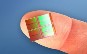
Intel and Micron plan to have samples of a 128Gbit 3D crosspoint memory by the end of the year with commercial shipments in 2016.

Intel claims that the new memory, which it calls XPoint, writes ‘up to 1000 faster than NAND’ and has 1000 times the endurance of NAND.

The memory has a cross point array structure described, in the press release, as a “3D checkerboard where memory cells sit at the intersection of word lines and bit lines, allowing the cells to be addressed individually. As a result, data can be written and read in small sizes, leading to faster and more efficient read/write processes.”

The release adds:

“More details about 3D XPoint technology include:

Cross Point Array Structure – Perpendicular conductors connect 128 billion densely packed memory cells. Each memory cell stores a single bit of data. This compact structure results in high performance and high-density bits.

Stackable – In addition to the tight cross point array structure, memory cells are stacked in multiple layers. The initial technology stores 128Gb per die across two memory layers. Future generations of this technology can increase the number of memory layers, in addition to traditional lithographic pitch scaling, further improving system capacities.

Selector – Memory cells are accessed and written or read by varying the amount of voltage sent to each selector. This eliminates the need for transistors, increasing capacity while reducing cost.”

david manners