Author Archives: david manners

Qualcomm buys Ikanos

Qualcomm sales officeQualcomm is to buy Ikanos for $47 million to expand its broadband and modem portfolio for fixed line consumer business.

It will help provide, says Qualcomm: ‘a central hub for Internet of Everything (IoE) enabled devices, services and 3G/LTE small cells.’

“Qualcomm Atheros has always viewed the home gateway as the enabler for consumers to not only access the Internet for browsing and downloading content and video streaming, but also as the hub of the Internet in the home for a variety of reliable and high quality services,” says Qualcomm’s Rahul Patel, “the combination of Qualcomm Atheros’ broad home gateway IP portfolio, including Wi-Fi, powerline, small cell, and Ethernet switch technologies, and Ikanos’ advanced wired modem technology, is designed to create a complete solution for a wide range of home gateway products to better serve the carrier segment.”

What Ikanos brings to Qualcomm is: A/VDSL2 and G.fast modem technology and chipsets for consumer premises equipment (CPE) and central office (CO) infrastructure; multi-mode gateway processor and accelerator technology for fibre, LTE, Ethernet and hybrid-copper applications; Ikanos’ inSIGHT software for remote diagnosis, management and optimisation of the broadband connection and quality-of-service, and VoIP integrated access devices and bridges.

More Qualcomm stories on Electronics Weekly raquo

david manners

How to measure the productivity of your R&D dollar

26aug15Dundon, Gerald, ADIThere are two main difficulties about measuring the productivity of R&D: one is the length of time from initial spend to the moment the last sales dollar is delivered; the other is the difficulty of associating inputs to outputs – how do we know that what is discovered in the R&D process has led to the creation of a saleable product?

Thirty-year Analog Devices’ veteran Gerald Dundon has cracked this very tough nut in a book called R&D Productivity: How to target it. How to measure it. Why it matters.

At ADI, Dundon held the jobs of vice-president of supply chain and planning, vice-president of quality, and vice-president of new product productivity.

You would think the amount of revenue coming from new products is a valid metric for R&D efficiency but you would be wrong, says Dundon.

He regards discounted cash flow as an inadequate metric for R&D project evaluation.

He explains why R&D spend should be included in return-rate calculations, how cumulative revenue can be modelled and predicted and how product lifecycles influence target rate returns – too short a product lifecycle means you’re ‘living on the edge’, says Dundon.

This is a heavyweight book for semiconductor management and it answers one of the most difficult questions the industry has to face: how do you create a business out of R&D.


david manners

Diablo puts flash into servers

Diablo CEO Riccardo Badalone

Diablo CEO Riccardo Badalone

Diablo Technologies’ Memory1, an all-flash server system memory technology, puts 4TBytes of memory in slots that currently hold 128Gbytes or 384Gbytes, the company said.

By delivering greater capability on fewer servers it claims to reduce data centre costs by up to 70%.

Memory1 is shipping now to select customers and will be more widely available later in the year.

“Memory1 represents a major evolution in server architecture,” says Diablo CEO Riccardo Badalone. “The needs of the large-scale datacenter are changing, with a very sharp focus on increasing capability to win the internet while managing tight constraints on cost and power. The Memory1 platform allows customers to leverage NAND flash as pure system memory in a seamless manner, with no changes to their hardware and software stacks. The business impact on datacentre economics and application performance is dramatic. We’ve seen customers envisioning everything from aggressive server consolidation all the way to doubling and tripling individual machine profit.”

Memory1 brings the low cost and high capacity of flash to large-scale enterprise and datacenter customers, he said. It is suitable for environments that require large memory footprints per server for workloads, such as big data analytics and complex web applications.

The average Memory1 use case enables a four-to-one server reduction, and one customer use case requires 90% fewer servers.

Diablo will initially focus on delivering Memory1 to cloud and hyperscale datacenters, which stand to see significant economic benefits because of their scale.

david manners

Diablo puts flash into servers

Diablo CEO Riccardo Badalone

Diablo CEO Riccardo Badalone

Diablo Technologies’ Memory1, an all-flash server system memory technology, puts 4TBytes of memory in slots that currently hold 128Gbytes or 384Gbytes, the company said.

By delivering greater capability on fewer servers it claims to reduce datacentre costs by up to 70%.

Memory1 is shipping now to select customers and will be more widely available later in the year.

“Memory1 represents a major evolution in server architecture,” says Diablo CEO Riccardo Badalone. “The needs of the large-scale datacenter are changing, with a very sharp focus on increasing capability to win the internet while managing tight constraints on cost and power. The Memory1 platform allows customers to leverage NAND flash as pure system memory in a seamless manner, with no changes to their hardware and software stacks. The business impact on datacentre economics and application performance is dramatic. We’ve seen customers envisioning everything from aggressive server consolidation all the way to doubling and tripling individual machine profit.”

Memory1 brings the low cost and high capacity of flash to large-scale enterprise and datacenter customers, he said. It is suitable for environments that require large memory footprints per server for workloads, such as big data analytics and complex web applications.

The average Memory1 use case enables a four-to-one server reduction, and one customer use case requires 90% fewer servers.

Diablo will initially focus on delivering Memory1 to cloud and hyperscale datacenters, which stand to see significant economic benefits because of their scale.

david manners

Plessey selling GaN-on-Si LED die

Plessey 4.5mm high power die

Plessey 4.5mm high power die

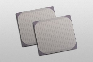
Today Plessey announced the release of its range of GaN-on-Si MaGIC LED die.

The blue die, sometimes referred to as blue pump for their ability to pump phosphor to a white colour range, are the latest innovation in high brightness LED die designed for a wide range of medium to high power applications including general lighting, signage, commercial, residential and street lighting.

“We have developed a wide range of LED die for a number of applications and our GaN-on-Silicon technology works particularly well in higher power applications such as high bay, street lights, projector lamps, spot lamps and floodlighting,” says Plessey CTO Keith Strickland. “This process technology will become the base for our application-specific LEDs, the ASLED, which bridges the gap between LED component suppliers, solid state lighting fixture designers and the OEMs.”

The manufacturing process produces a vertical LED structure which has the anode as bottom contact and the cathode formed in the top metal layer. The layout of the top metal layer is optimised for a particular LED size and die operating current, and includes one or more bond pads for connecting to the cathode.

Plessey offers its range of blue die in various wavelength options. Capable of generating over 60% light output efficiency, sometimes referred to as wall plug efficiency (WPE), the die are supplied to a standard thickness of 150μm, while other thicknesses can be supplied, down to a minimum of 75μm.

The die are supplied on a blue tape in single intensity and colour bins to provide close uniformity, and are intended to be used with standard pick and place machines.

Samples are available in a variety of die pack formats with blue die wavelengths ranging from 420nm to 480nm and from mW to 10W with the PExS4500 range having a typical optical output power of 4000mW from a 3A drive current.

david manners

Plessey selling GaN-on-Si LED die


Plessey's GaN-on-Silicon MaGIC LED die

Plessey’s GaN-on-Silicon MaGIC LED die

Today Plessey announced the release of its range of GaN-on-Silicon MaGIC LED die.

The blue die, sometimes referred to as blue pump for their ability to pump phosphor to a white colour range, are the latest innovation in high brightness LED die designed for a wide range of medium to high power applications including general lighting, signage, commercial, residential and street lighting.

“We have developed a wide range of LED die for a number of applications and our GaN-on-Silicon technology works particularly well in higher power applications such as high bay, street lights, projector lamps, spot lamps and floodlighting,” says Plessey CTO Keith Strickland. “This process technology will become the base for our application-specific LEDs, the ASLED, which bridges the gap between LED component suppliers, solid state lighting fixture designers and the OEMs.”

The manufacturing process produces a vertical LED structure which has the anode as bottom contact and the cathode formed in the top metal layer. The layout of the top metal layer is optimised for a particular LED size and die operating current, and includes one or more bond pads for connecting to the cathode.

Plessey offers its range of blue die in various wavelength options. Capable of generating over 60% light output efficiency, sometimes referred to as wall plug efficiency (WPE), the die are supplied to a standard thickness of 150μm, while other thicknesses can be supplied, down to a minimum of 75μm.

The die are supplied on a blue tape in single intensity and colour bins to provide close uniformity, and are intended to be used with standard pick and place machines.

Samples are available in a variety of die pack formats with blue die wavelengths ranging from 420nm to 480nm and from mW to 10W with the PExS4500 range having a typical optical output power of 4000mW from a 3A drive current.

david manners

Semiconductor sales see record Q2, says SIA

June 2015-SIA-graph-semi-salesQ2 semi sales rose 1% over Q1 and 2% over Q2 2014 to reach an all-time sales record for Q2 of $84 billion, reports the Semiconductor Industry Association (SIA).

June sales were down 0.4% on May but up 2% on June 2014 reaching $28bn.

Year-to-date sales are 3.9% higher than last year.

“Macroeconomic headwinds and softening demand have slowed global semiconductor market growth somewhat, but the industry still posted its highest-ever second-quarter sales and remains ahead of the pace of sales set in 2014, which was a record year for semiconductor revenues,” says SIA CEO John Neuffer. “The Americas market continues to post solid year-to-year sales increases, and the global market has now grown on a year-to-year basis for 26 consecutive months.”

Regionally, sales increased compared to June 2014 in China (7.8%), the Americas (5.6%), and Asia Pacific/All Other (5.2%), but fell in Europe (-11.5%) and Japan (-13.6%).

Sales were up slightly compared to last month in Japan (1.0%) and China (0.6%), but down somewhat in Asia Pacific/All Other (-0.6%), the Americas (-1.6%), and Europe (-1.7%).

Sales figures in Europe and Japan have been affected by currency devaluation.

“Global semiconductor sales are one indicator of the strength of the US industry, which accounts for more than half of total global sales,” says Neuffer.

david manners

China semiconductor sales worth $12.5bn last year – CSIA

TI China fabChina’s semiconductor industry value chain was worth $48 billion last year, according to the China Semiconductor Industry Association (CSIA) but is largely contributed by foreign companies.

The output value of the China semiconductor industry was $12.5bn in 2014, of which $5bn came from IC design, $3.7bn from fabrication, and $3.8bn from packaging and testing.

80% of the wafers produced in China came from TSMC, says the CSIA.

The China government is investing heavily to create an indigenous memory industry, says the CSIA, because China is the largest memory market and buys 75% of global memory production.

See more China stories on Electronics Weekly »

david manners