Author Archives: david manners

Low phase noise oscillator from Crystek

Crystek CCPD-575 - an Ultra-Low Phase Noise LVPECL Oscillator

Crystek CCPD-575 – an Ultra-Low Phase Noise LVPECL Oscillator

Crystek has launched the CCPD-575 – an Ultra-Low Phase Noise LVPECL Oscillator providing a -162 dBc/Hz noise floor.

The chip’s phase noise is claimed to be 15 dB lower phase noise than most LVPECL oscillators on the market.

Close-in phase noise i -90 dBc/Hz for the 100 MHz variant. This overall ultra-low phase noise translates to a typical phase jitter of 85 fS RMS (12 kHz to 20 MHz).

The low phase noise performance is useful in applications such as: Digital Video, SONET/SDH/DWDM, Storage Area Networks, Broadband Access, Ethernet, and Gigabit Ethernet.

CCPD-575
Frequency (MHz) 50.000 to 156.250
Package 5.0 x 7.5 mm SMD
Supply (VDC) 3.30
Output LVPECL
Stability ppm (°C) ±20 (-40 to 85)
P/N (dBc/Hz) -162 @ Floor
Data Sheet CCPD-575.pdf

david manners

IDT extends VVA frequency coverage

RF VVA - The F2255 and F2258 devices offer industry-leading low insertion loss and high linearity

RF VVA – The F2255 and F2258 devices offer industry-leading low insertion loss and high linearity

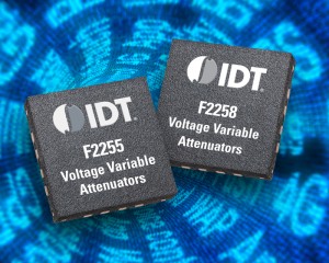
IDT has introduced two RF voltage variable attenuators (VVA) which expand its VVA frequency coverage to a range of 1 MHz to 6 GHz. Like the other members of the family, the F2255 and F2258 devices offer industry-leading low insertion loss and high linearity.

IDT’s VVAs deliver analogue control for applications that require precise attenuation. Both new devices come in a 3 millimeter by 3 millimeter, 16-pin TQFN package. They offer IP3 performance 1000x (30 dB) better than Gallium arsenide (GaAs) devices, and they exhibit a linear-in-dB attenuation characteristic across the voltage control range. Their low insertion loss reduces RF chain path loss, while their high linearity improves system data rates.

These newest devices match popular footprints and are suitable for base stations (2G, 3G and 4G), microwave infrastructure, public safety, portable wireless communication/data equipment, test/ATE equipment, military systems, JTRS radios, and HF, VHF and UHF radios.

By using silicon-based RF semiconductor technology, IDT’s attenuators offer an alternative to GaAs-based semiconductor technology. Silicon technology offers the advantages of improved RF performance as well as more robust electrostatic discharge (ESD) protections, better moisture sensitivity levels (MSL), improved thermal performance, lower current consumption, and the proven reliability of silicon technology.

Comparing the F2258 to its pin-compatible GaAs competitor, the device has an Input IP3 of up to 65dBm vs 35dBm, a maximum attenuation slope of 33dB/Volt vs. 53dB/Volt; minimum return loss up to 6000MHz, 12.5dB vs. 7dB; and operating maximum temperature range of 105C Vs 85C. The F2255 device supports a frequency range down to 1MHz and has a maximum attenuation slope of 33dB/Volt. Both devices have bi-directional RF ports, support a single positive supply voltage of either 3V or 5V and have an operating temperature range of -40 to 105C.

david manners

Flash-based storage start-up Pure going for IPO

Flash-based storage start-up Pure going for IPO

Flash-based storage start-up Pure going for IPO

Loss-making flash-based storage company Pure Storage has filed for an IPO.

Last year the company lost $182 million on sales of $174 million.

According to IDC, Pure is the second largest supplier of flash-based storage behind EMC and ahead of IBM and HP.

The market for all-flash storage systems was $1.6 billion last year and will be $2.24 billion this year, says IDC.

Pure’s losses were $23.4 million in 2013, $78.6 million in 2014 and $183.2 million in 2015. For the three months to April 2025, it lost $49.1 million.

Revenues were $6.1 million in 2013, $42.7 million in 2014 and $174.5 million in 2015. For the three months to April 30, 2015, revenues were $74.1 million.

Pure has had $531 million in investment capital. It wants to raise $300 million in the IPO, valuing the company at $3 billion.

The overall storage market, dominated by hard disk, is worth $26.5 billion.

Top Seven Flash-based Storage players are:

  • EMC
  • Pure
  • IBM
  • NetApp
  • HP
  • SoldFire
  • Nimbus

Source: IDC


david manners

Samsung starts production of 48-layer V-NAND

Samsung begins mass production of 48-layer three-bit-per-cell 256Gbit V-NAND

Samsung begins mass production of 48-layer three-bit-per-cell 256Gbit V-NAND

Samsung says it has begun mass production of 48-layer three-bit-per-cell 256Gbit V-NAND.

Last week Toshiba said it was beginning pilot production of a 48-layer 256Gbit 3 bit-per-cell V-NAND, which it calls BiCS Flash.

In March, Intel/Micron said they were starting to ship a 32-layer V-NAND using floating point flash technology which delivered a 256Gbit memory.

Since then Intel/Micron have also announced their mystery memory technology 3D XPoint which may sample later this year.

Samsung’s 48-layer memory uses charge trap technology. The chip has 85.3 billion cells, which can store three bits each.

The 48-layer device uses 30% less power than the 32-layer, 128Gb V-NAND device when storing the same amount of data, and is 40% cheaper to make in terms of cost per storage bit.

See more Samsung Electronics stories on Electronics Weekly »

david manners

Electronic DC load returns 94% of load test energy to the grid

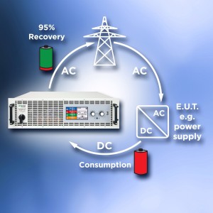
imageIntepro Systems has brought out electronic DC loads with an integral, grid-synchronized inverter designed to return up to 94% of the load test energy back to the grid.

The rack-mounted unit has output ratings of 3.5 kW, 7 kW and 10.5 kW — scalable to 105 kW. It costs $8000 and is available on an 8-12 week lead-time.

The ELR9000 Series offers four common regulation modes: constant voltage, constant current, constant resistance and constant power. The FPGA-based operational controls include a function generator and a table-based regulation circuit for the simulation of non-linear internal resistances.

Intepro’s PowerStar 6 software package enables the creation of test routines using a drag-and-drop menu where coding can be performed without programming.

“Our ELR9000 Series of electronic DC loads offers all the necessary features of today’s electronic loads — plus the added benefit of energy recovery to mains,” says Intepro CTO Gerard Sheehan, ‘recovering the load energy reduces energy costs. It also offers a cost-effective alternative to the expensive cooling systems used by conventional air- and water-cooled loads to dissipate energy as heat.”

david manners

Toshiba to sample fast SSDs

In Q4, Toshiba is to sample three new families of SSDs with high-speed PCIe interfaces that provide high-bandwidth point-to-point links with the processor and reduce system bottlenecks. 6741A_HRES

The drives use the NVMe protocol and have been designed for various applications including high performance notebooks, thin notebooks, 2-in-1/convertible notebooks, all-in-one PCs and tablets; and server and storage applications.

Each SSD family has been engineered to provide optimum performance and reliability for its target application with capacity, form-factor and security capabilities to match. All three SSD families make use of Toshiba-developed controller platforms and Toshiba’s own state-of-the-art MLC NAND flash memory.

The XG3 family of SSDs is housed in M.2 Type 2280 form factor and is the industry’s highest capacity[1] (1024GB[2]) client NVMe SSD designed for high performance notebooks, 2-in-1 laptop and all-in-one PCs. The drives support up to four lanes of PCIe 3.1, which has a maximum interface bandwidth more than six times that of SATA 6.0 Gbits/s[3]. The XG3 is also the industry’s first[1] NVMe SSD available in a 2.5-inch SATA express form factor.

The XG3 SSD family is equipped with Toshiba’s QSBC (Quadruple Swing-By Code) error-correction technology, a highly efficient error correction code (ECC), which helps protect customer data from corruption, improves reliability, and extends the life of Toshiba SSDs. Engineered for power efficiency, the XG3 series also features lower power state modes and is the first Toshiba product, along with the BG1 SSD family, to support the Trusted Computing Group security specification, Pyrite (TCG Pyrite).

The BG1 SSD family is the world’s smallest[1] NVMe SSD, available in a single package measuring just 16mm x 20mm (M.2 Type 1620) or a removable M.2 Type 2230 module with up to 256GB in capacity. Designed for thin notebooks, 2-in-1/convertible notebooks and tablets, the BG1 family enables PC OEMs to produce thin mobile PCs and tablets while offering a better performing alternative over SATA SSDs for mobile PCs. The BG1 SSD family supports TCG Pyrite and features lower power state modes.

The PX04P series of enterprise SSDs are designed for servers and storage appliances needing scalable power and performance settings. The PX04P series NVMe SSD has the industry’s lowest power consumption[1], with only 18 Watts needed to power the drive at maximum performance. PX04P’s combined high performance and low power consumption may contribute to low total cost of ownership demanded by today’s enterprise data centers. The PX04P family also supports up to four lanes of PCIe 3.0, and is available in either a HHHL (half-height half-length) add-in card or a 2.5-inch form factor with SFF-8639 connector. The eSSD family is also equipped with Toshiba’s QSBC error-correction technology.

david manners

Silicon Labs enables clock-tree-on-a-chip

SLAB0276_Si5348-press-image-no-textSilicon Labs claims best-in-class jitter performance for its Si5348 clock IC which enables hardware designers to implement a “clock-tree-on-a-chip” solution for Synchronous Ethernet (SyncE), IEEE 1588v2 and general-purpose frequency translation for wireless and telecom infrastructure, broadband networks (e.g., G.fast DSL and PON) and data centre applications.

SyncE and IEEE 1588 have become increasingly popular methods to deliver synchronization over packet networks. As these technologies become more widespread, networking equipment designers are demanding more flexible, cost-effective timing solutions that easily integrate into existing hardware architectures. Conventional network synchronizer clocks rely on rigid synchronization clock chip architectures that borrow heavily from legacy Stratum 3 clock ICs, which are not optimized for size, power or performance.

The Si5348 clock delivers a solution that claims to be 50% smaller, 35% lower power and 80% lower jitter than conventional synchronizers delivering a timing solution compliant with IEEE 1588, SyncE and Stratum 3 clocking requirements, enabling the device to be used in a wide variety of timing card and line card clock architectures. The Si5348 clock has been designed to interoperate with IEEE 1588 software running on an external host processor, further simplifying system integration.

In packet timing applications, high-stability oscillators play a critical role in defining the network’s overall performance in terms of frequency, time and phase accuracy. Network topologies often will dictate the type of temperature-controlled crystal oscillator (TCXO) or oven-controlled crystal oscillator (OCXO) required at each node in the network. The Si5348 clock supports a universal reference input port, enabling the device to be paired with any frequency TCXO/OCXO.

Silicon Labs has partnered with Rakon to deliver a combined solution that can be used across a variety of SyncE and IEEE 1588 applications.

Factory pre-programmed samples and production quantities of the Si5348 network synchronizer clock are available now in a 9 mm x 9 mm QFN package. Si5348 pricing in 10,000-unit quantities ranges from $10.00 to $12.00 (USD), depending on output frequency. Silicon Labs’ Si5348-EVB evaluation board, priced at $399 (USD MSRP), enables developers to move quickly from device configuration to detailed performance analysis to custom part number generation in less than five minutes.

david manners

Record silicon wafer area shipments in Q2

SEMI silicon shipments 2015

Worldwide silicon wafer area shipments increased during Q2 2015

Worldwide silicon wafer area shipments increased during Q2 2015 compared to Q1, says the SEMI Silicon Manufacturers Group (SMG).

Total silicon wafer area shipments were 2,702 million square inches during the most recent quarter, a 2.5% increase from the 2,637 million square inches shipped during the previous quarter resulting in a new quarterly volume shipment record, says SEMI’s Silicon Manufacturers” Group.

New quarterly total area shipments are 4.4% higher than second quarter 2014 shipments. First half 2015 shipments are 7.8% higher than the first half of 2014.

“For two consecutive quarters, strong silicon shipment growth has been recorded by the Silicon Manufacturers Group,” says Ginji Yada, chairman of SEMI SMG and general manager, International Sales & Marketing Department of SUMCO Corporation, “continued growth off of the record level shipped in the first quarter, produced another record level of shipments in the most recent quarter.”

The increasing level of silicon shipped since Q2 last year, measured in million square inches is:

Q2 2014 – 2,587, Q1 – 2015 – 2,637, Q2 2015 – 2,702, H1 – 4,951, H2 2015 – 5,339.

View previous SEMI reports on Electronics Weekly »

SEMI is a global industry association serving the nano- and micro-electronic manufacturing supply chains with 1,900 member companies.

See alsoSEMI book-to-bill languishes


david manners