Author Archives: david manners

Toshiba expands backside illumination CMOS sensor range

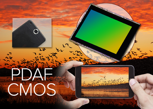
Toshiba has expanded its range of backside illumination CMOS image sensors equipped with Phase Detection Auto-Focus (PDAF).

Designed for use in smartphones and tablets the sensors achieve high performance image capture and low power consumption.

toshyThe range expansion features the 8 megapixel (MP) T4KA3-121, the 16 MP T4KC3-121, the 13 MP T4KB3-121 and the 20 MP T4KA7-121.

Originally developed for SLR cameras, PDAF locks in focus at speeds much faster than the auto-focus systems currently used in smartphones and tablets – making it easier for mobile devices to capture not only the still objects, but also fast moving objects.

Image brightness is boosted by up to four times by Toshiba’s Bright Mode technology and the sensors also support high dynamic range (HDR) to capture natural images of scenes with a high contrast ratio, ending the problem of over- and underexposed images.

Mobile device manufacturers are constantly striving to design and build the most powerful, power efficient devices in the smallest possible form-factors. In order to support this need for smaller components, Toshiba has developed a design method that realises smaller CMOS sensor chips and low-power circuits.

The T4KA3-121 achieves output speeds of up to 30fps at full 8MP-resolution – with power consumption figures of just 140mW or lower. Full-HD outputs are supported at frame rates of up to 60fps, and HD outputs are supported at 120fps in normal mode and 240fps in Bright Mode.

The T4KB3-121 and T4KC3-121 achieve output speeds of up to 30fps at 4K2K resolutions, Full-HD at frame rates of up to 60fps, and HD outputs at 120fps.

The T4KA7-121 achieves output speeds of up to 22ps at full 20MP-resolution 24fps at 18.8MP and 28fps at 16.3MP, with a power consumption of 440mW.

david manners

Marvell gets AT&T validation for LTE multimode chip-set

Marvell PXA1908, smart meters

Marvell PXA1908

Marvell’s Armada PXA1928 and PXA1908 mobile multi-mode LTE chip-sets have completed the AT&T ADAPT validation process for multi-mode LTE data and voice services.

Marvell co-founder and president Weili Dai described them as “best-in-class LTE single chip solutions”, for “cost-effective and field-proven smart devices”.

Both Marvell’s PXA1928 and PXA1908 achieved compliance to AT&T’s device requirements and interoperability on AT&T’s network, along with VoLTE, and as a result were granted ADAPT Validation Complete (AVC) status.

The Armada Mobile PXA1928 SoC incorporates the performance of the quad-core ARM Cortex-A53 running at 1.5GHz with Marvell’s five-mode modem technology to provide a cost effective Android mobile platform. It supports 2G/3G/4G communications and enables a breakthrough end-user experience for high-end multimedia and gaming applications.

Armada Mobile PXA1908, Marell’s second quad-core 64-bit five-mode LTE SoC, which is designed to enable easy integration from 2G/3G to 4G LTE connectivity.

In addition to the cost-optimised quad-core Cortex-A53 with up to 1.5GHz clock speed, PXA1908 offers improved image processing to support 8MP camera sensors, advanced power management, integrated location and sensor hub functions.

david manners

Toshiba shipping wireless charger IC

imageToshiba is shipping a wireless power receiver IC that will enable mobile devices to be charged wirelessly as fast as if they were connected to the charger via a cable.

The TC7764WBG is compliant with Qi V.1.1.2, the wireless low power charging standard defined by the Wireless Power Consortium (WPC), which includes a dedicated specification for smartphones and mobile accessories.

Wireless charging allows adoption of a fully insulated case free of exposed charging ports, an advantage that is stimulating demand for waterproof and dustproof smartphones and other mobile devices. However, wireless charging has not always been as fast as charging by cable.

Toshiba has addressed this problem by optimizing the circuit design of the TC7764WBG compared to its predecessor products, enabling maximum output power of 5W and maximum power conversion efficiency of 95 percent1. This will allow wireless charger makers utilizing the new IC to achieve performance as fast as that offered by cabled chargers, with added benefits.

To ensure mobile device safety, the new IC integrates a protocol authentication circuit for power transfers, foreign object detection functions, under-voltage lockout (UVLO) and over voltage detection (OVLO) functions, as well as thermal shutdown function (TSD). The IC is housed in a WCSP28 package measuring 2.4mm by 3.67mm by 0.5mm.

david manners

Rambus goes fabless

Rambus is going fabless. After 25 years as an IP supplier it will start selling ICs under its own name.

The first products will be for communications in data centres and will be on sale by the end of the year.

Data buffers are expected to be among the the first products.

Rambus has had to resort to extensive and expensive litigation to enforce its IP and has got into trouble with the FTC for allegedly rigging standards.

See alsoHynix and Rambus agree nine year licensing deal

See alsoKey Rambus patent invalidated by US Patent Office


david manners

Kemet launches mission critical capacitors

imageKemet has launched its M55 Module Polymer Hermetic Seal (PHS) capacitor portfolio designed for mission critical high capacitance and voltage applications.

They are manufactured by placing T550 or T551 Polymer Hermetic Seal capacitors in parallel. The M55 Series is suitable for telecom, computer, defence and aerospace applications.

With its robust anode quality, benign failure mode, mechanically robust assembly and epoxy housing, the M55 Series of modules are ideal for use in high voltage power management applications such as buck boost converters, filtering, hold-up capacitors, and other high ripple or high in-rush current applications.

The M55 Modular Series provides extremely low and stable ESR and enhanced capacitance retention at higher frequencies and low temperatures, resulting in the highest total capacitance and most economical solution for high power applications.

The supplier has qualified the discrete components used in the M55 Series to DLA Drawing 13030 to ensure these products are suitable for high reliability applications Kemet, in association with entities within the space community and several Kemet aerospace customers, has confirmed that the rigorous testing options included in this comprehensive drawing are applicable to standard and high reliability flight applications including space. Discrete parts qualified according this drawing are available options for this modular capacitance solution.

The M551 Series offers all of the performance benefits of the M550 Series but with an increased temperature rating of 125 degrees Celsius. The M550 modular series is rated at 105 degrees Celsius.

david manners

Imec extends GaN-on-Si R&D programme

imageImec is extending GaN-on-Si R&D programme to offer joint research on GaN-on-Si 200mm epitaxy and enhancement-mode device technology.

The extended R&D initiative includes exploration of novel substrates to improve the quality of the epitaxial layers, new isolation modules to increase the level of integration, and the development of advanced vertical devices.

Imec says that it welcomes new partners interested in next-generation GaN technologies and companies looking for low-volume manufacturing of GaN-on-Si devices to enable the next generation of more efficient and compact power converters.

GaN technology offers faster-switching power devices with higher breakdown voltage and lower on-resistance than silicon, making it an outstanding material for advanced power electronic components. Imec’s R&D program on GaN-on-Si was launched to develop a GaN-on-Si process and bring GaN technology towards industrialization.

“Since the program’s launch in July 2009, we have benefited from strong industry engagement, including participation from integrated device manufacturers (IDMs), epi-vendors and equipment and material suppliers. This underscores the industrial relevance of our offering,” says Imec’s Rudi Cartuyvels.

Building on its track record in GaN epilayer growth, new device concepts and CMOS device integration, Imec has now developed a complete 200mm CMOS-compatible GaN process line. Imec’s GaN-on-Si technology is reaching maturity, and companies can gain access to the platform by joining its GaN-on-Si industrial affiliation program (IIAP).

The process line is also open to fabless companies interested in low-volume production of GaN-on-Si devices tailored to their specific needs, through dedicated development projects.

Imec’s portfolio includes three types of buffers optimized for breakdown voltage and low trap-related phenomena (i.e. current dispersion):

a step-graded aluminium gallium nitride (AlGaN) buffer;

a superlattice buffer;

a buffer with low-temperature AlN interlayers.

Imec explored side-by-side enhancement-mode power devices of the MISHEMT and p-GaN HEMT type, as well as a gate-edge-terminated Schottky power diode featuring low reverse leakage and low turn-on voltage.

The latest generation of Imec enhancement-mode power devices shows a threshold voltage beyond +2V, an on-resistance below 10 ohm mm and output current beyond 450mA/mm. These devices represents the state-of-the-art of enhancement-mode power devices, Imec claims.

In this next phase of the GaN program, Imec is focusing on further improving the performance and reliability of its existing power devices, while in parallel pushing the boundaries of the technology through innovation in substrate technology, higher levels of integration and exploration of novel device architectures.

“Interested companies are invited to become a partner and actively participate in our program,” says Cartuyvels. “Imec’s open innovation model allows companies to have early access to next-generation devices and power electronics processes, equipment and technologies and speed up innovation at shared cost.”

david manners

Imec extends GaN-on-Si R&D programme

imageImec is extending GaN-on-Si R&D programme to offer joint research on GaN-on-Si 200mm epitaxy and enhancement-mode device technology.

The extended R&D initiative includes exploration of novel substrates to improve the quality of the epitaxial layers, new isolation modules to increase the level of integration, and the development of advanced vertical devices.

Imec says that it welcomes new partners interested in next-generation GaN technologies and companies looking for low-volume manufacturing of GaN-on-Si devices to enable the next generation of more efficient and compact power converters.

GaN technology offers faster-switching power devices with higher breakdown voltage and lower on-resistance than silicon, making it an outstanding material for advanced power electronic components. Imec’s R&D program on GaN-on-Si was launched to develop a GaN-on-Si process and bring GaN technology towards industrialization.

“Since the program’s launch in July 2009, we have benefited from strong industry engagement, including participation from integrated device manufacturers (IDMs), epi-vendors and equipment and material suppliers. This underscores the industrial relevance of our offering,” says Imec’s Rudi Cartuyvels.

Building on its track record in GaN epilayer growth, new device concepts and CMOS device integration, Imec has now developed a complete 200mm CMOS-compatible GaN process line. Imec’s GaN-on-Si technology is reaching maturity, and companies can gain access to the platform by joining its GaN-on-Si industrial affiliation program (IIAP).

The process line is also open to fabless companies interested in low-volume production of GaN-on-Si devices tailored to their specific needs, through dedicated development projects.

Imec’s portfolio includes three types of buffers optimized for breakdown voltage and low trap-related phenomena (i.e. current dispersion):

a step-graded aluminium gallium nitride (AlGaN) buffer;

a superlattice buffer;

a buffer with low-temperature AlN interlayers.

Imec explored side-by-side enhancement-mode power devices of the MISHEMT and p-GaN HEMT type, as well as a gate-edge-terminated Schottky power diode featuring low reverse leakage and low turn-on voltage.

The latest generation of Imec enhancement-mode power devices shows a threshold voltage beyond +2V, an on-resistance below 10 ohm mm and output current beyond 450mA/mm. These devices represents the state-of-the-art of enhancement-mode power devices, Imec claims.

In this next phase of the GaN program, Imec is focusing on further improving the performance and reliability of its existing power devices, while in parallel pushing the boundaries of the technology through innovation in substrate technology, higher levels of integration and exploration of novel device architectures. 

“Interested companies are invited to become a partner and actively participate in our program,” says Cartuyvels. “Imec’s open innovation model allows companies to have early access to next-generation devices and power electronics processes, equipment and technologies and speed up innovation at shared cost.”

david manners

Gloomy Applied

CEO Gary Dickerson

CEO Gary Dickerson

Applied Materials has delivered a ‘flat to down’ forecast for calendar Q3 saying that the foundries are being cautious about spending because of high inventories.

Applied reported a 10% rise in its calendar Q2 revenue and a 17% rise in orders.

It saw calendar Q2 profits rise 9% to $329 million, and Q2 revenues rise to to $2.49 billion from $2.27 billion a year earlier.

For the current quarter, the company expects sales to be flat to down 7% from the previous quarter.

“Applied is focused on profitable growth and the results show in our third-quarter performance when we delivered our highest ever 300mm semiconductor equipment orders and record revenue in services,” says Applied CEO Gary Dickerson, “our highly differentiated materials engineering products help customers accelerate major technology inflections including 3D NAND, and this quarter we generated the highest flash memory orders in our history.”

applied Q3

See more Applied Materials stories on Electronics Weekly »

david manners