Author Archives: david manners

LAPIS sampling 10-cell li-ion battery monitoring IC

LAPIS is sampling a 10-cell lithium-ion battery monitoring LSI that provides a current consumption of 25μA

LAPIS is sampling a 10-cell lithium-ion battery monitoring LSI that provides a current consumption of 25μA

LAPIS Semiconductor, a part of ROHM, is sampling a 10-cell lithium-ion battery monitoring LSI that provides a current consumption of 25μA (typ.) making it suitable for battery protection systems in cordless vacuum cleaners, electric tools, and other portable equipment.

The ML5233 has 0.1μA (typ.) current consumption during power down, minimising the effects on battery capacity – even during long-term storage – and contributing to more eco-friendly products with virtually no loss of charged battery power.

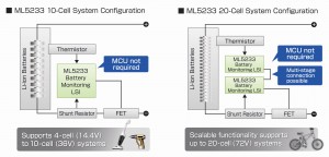
In addition, built-in temperature and short-circuit current detection circuits enable detection of not only over-charge/discharge and overcurrent, but also abnormal (high) temperatures during discharge along with battery pack short-circuits – all without an MCU. This decreases footprint by 20% and reduces the number of external components from four to one, leading to smaller battery protection systems and lighter development load.

Overcharge detection accuracy (±15mV per each cell) increases charging efficiency by 7% over products with ±50mV accuracy.

High-voltage processes support 4-10 cells in series using a single LSI, ensuring compatibility with electric tools and other equipment in the 14V to 36V range.

Two LSIs can be combined to support up 20 cells in series and up to 72V.

The company writes:

The ML5233 is a protection IC for the 4- to 10-cell Li-ion rechargeable battery pack. It detects individual cell overvoltage/undervoltage and the pack overcurrent/over-temperature, and then automatically controls the ON/OFF state of the external charge/discharge NMOS-FETs accordingly. Also the ML5233 can be cascaded to handle battery packs with more than 10 cells.

See also: French firm wins Lapis Semi Bluetooth antenna design in


david manners

LAPIS sampling 10-cell li-ion battery monitoring IC

LAPIS is sampling a 10-cell lithium-ion battery monitoring LSI that provides a current consumption of 25μA

LAPIS is sampling a 10-cell lithium-ion battery monitoring LSI that provides a current consumption of 25μA

LAPIS Semiconductor, a part of ROHM, is sampling a 10-cell lithium-ion battery monitoring LSI that provides a current consumption of 25μA (typ.) making it suitable for battery protection systems in cordless vacuum cleaners, electric tools, and other portable equipment.

The ML5233 has 0.1μA (typ.) current consumption during power down, minimising the effects on battery capacity – even during long-term storage – and contributing to more eco-friendly products with virtually no loss of charged battery power.

In addition, built-in temperature and short-circuit current detection circuits enable detection of not only over-charge/discharge and overcurrent, but also abnormal (high) temperatures during discharge along with battery pack short-circuits – all without an MCU. This decreases footprint by 20% and reduces the number of external components from four to one, leading to smaller battery protection systems and lighter development load.

Overcharge detection accuracy (±15mV per each cell) increases charging efficiency by 7% over products with ±50mV accuracy.

High-voltage processes support 4-10 cells in series using a single LSI, ensuring compatibility with electric tools and other equipment in the 14V to 36V range.

Two LSIs can be combined to support up 20 cells in series and up to 72V.

The company writes:

The ML5233 is a protection IC for the 4- to 10-cell Li-ion rechargeable battery pack. It detects individual cell overvoltage/undervoltage and the pack overcurrent/over-temperature, and then automatically controls the ON/OFF state of the external charge/discharge NMOS-FETs accordingly. Also the ML5233 can be cascaded to handle battery packs with more than 10 cells.

See also: French firm wins Lapis Semi Bluetooth antenna design in
 

david manners

LAPIS sampling 10-cell li-ion battery monitoring IC

LAPIS is sampling a 10-cell lithium-ion battery monitoring LSI that provides a current consumption of 25μA

LAPIS is sampling a 10-cell lithium-ion battery monitoring LSI that provides a current consumption of 25μA

LAPIS Semiconductor, a part of ROHM, is sampling a 10-cell lithium-ion battery monitoring LSI that provides a current consumption of 25μA (typ.) making it suitable for battery protection systems in cordless vacuum cleaners, electric tools, and other portable equipment.

The ML5233 has 0.1μA (typ.) current consumption during power down, minimising the effects on battery capacity – even during long-term storage – and contributing to more eco-friendly products with virtually no loss of charged battery power.

In addition, built-in temperature and short-circuit current detection circuits enable detection of not only over-charge/discharge and overcurrent, but also abnormal (high) temperatures during discharge along with battery pack short-circuits – all without an MCU. This decreases footprint by 20% and reduces the number of external components from four to one, leading to smaller battery protection systems and lighter development load.

Overcharge detection accuracy (±15mV per each cell) increases charging efficiency by 7% over products with ±50mV accuracy.

High-voltage processes support 4-10 cells in series using a single LSI, ensuring compatibility with electric tools and other equipment in the 14V to 36V range.

Two LSIs can be combined to support up 20 cells in series and up to 72V.

The company writes:

The ML5233 is a protection IC for the 4- to 10-cell Li-ion rechargeable battery pack. It detects individual cell overvoltage/undervoltage and the pack overcurrent/over-temperature, and then automatically controls the ON/OFF state of the external charge/discharge NMOS-FETs accordingly. Also the ML5233 can be cascaded to handle battery packs with more than 10 cells.

See also: French firm wins Lapis Semi Bluetooth antenna design in
 

david manners

Crystek launches 2.5GHz phase locked clock source

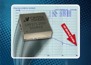
Crystek Microwave has launched a 2.5 GHZ phase locked clock source with internal reference, the CRFS75-2500

Crystek Microwave has launched a 2.5 GHZ phase locked clock source with internal reference, the CRFS75-2500

Crystek Microwave has launched a 2.5 GHZ phase locked clock source with internal reference, the CRFS75-2500 (.pdf).

The resulting source features -105dBc/Hz phase noise at 10KHz offset and a noise floor of -167dBc/Hz.

Crystek designed the module using proprietary circuitry and SAW (surface acoustic wave) resonator technology to provide ultra-low jitter/phase noise performance with true SineWave output.

CRFS75-2500
Frequency (MHz)
2500.000
Package 0.75 x 0.75 in
SMD
Supply (VDC) 5.00
Output SINEWAVE
Stability ppm (°C)
±25 (-20 to 70)
Data Sheet CRFS75-2500.pdf
Notes
  • Phase Locked


david manners

ERNI to launch 100G ATCA connectors

ERNI to launch 100G ATCA connectors

ERNI to launch 100G ATCA connectors

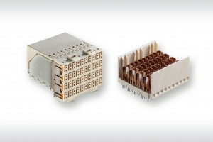
ERNI Electronics is to launch its ERmet ZDpro connector family for 100G ATCA systems next month.

This high-speed differential hard metric connector system enables data rates of >25 Gbit/s and claims to be the first connector system that meets the requirements for 100G ATCA technology.

The data rates and the improved transmission behaviour are mainly based on the reduced size of the signal termination, designed for vias with a diameter of only 0.30mm.

The drilling hole diameter for the shielding contacts is specified at 0.46mm. According to the company the fact that the reduction of the vias leads to an improved crosstalk behavior was the motivation to the further miniaturisation of the press-fit zone.

The communication technology shows an ongoing trend towards increasing data rates and higher bandwidths. This means there is a need for 100GbE (gigabit Ethernet) data transmission. Typical applications are the next generation of internet backbones, data centers or cloud computing.

ERmet ZDpro connectors fulfill the requirements and challenges of the interface between backplane and daughter cards in suchhigh speed systems, claims the company. The new product is based on the mechanical design of its ERmet ZD and ERmet ZDplus, with the same dimensions.

ERmet ZDpro connectors are backwards mating compatible to ERmet ZD and ZDplus connectors. This means that existing backplane designs do not need layout changes on the backplane side if customers want to upgrade their daughter cards in the first step before upgrading the whole system, although the layout on the daughter cards has to be modified, if ERmet ZDpro receptacles are used.

To benefit from the maximum performance of the ERmet ZDpro the company recommends backdrilling. Decreasing via stub length and the related “stub effect“ by backdrilling significantly reduces the reflections and the overall bit error rate of the connection.

The first products of the ERmet ZDpro family are the four-pair right-angle female connector and the related straight male connector with press-fit termination. Both will be available from September 2015.

The connectors provide 40 signal pairs. The male connectors are available with different contact lengths (3.8mm or 5.3mm). While the standard variants with 3.8mm contacts offer an optimised impedance behaviour the male connectors with 5.3mm contact lengths provide a 1.5mm higher wipe length of 2.9mm.

david manners

Three win Digi-Key/Silicon Labs IoT competition

The three winners of the "Your IoT Connected World" design contest have been announced

The three winners of the “Your IoT Connected World” design contest have been announced

Silicon Labs and Digi-Key have announced the three winners of the “Your IoT Connected World” design contest.

They are:

• Christian Klemetsson, who designed his “DeviceRadio” industrial automation solution to connect the real world to applications through virtual wires specifically within the industrial automation market. The goal of this product design is to deliver a custom IoT device on a solderless breadboard and controlled through the Internet in three minutes or less.

• Hoang Nhu, who developed a platform for extending the IoT through all parts of the home, from medication reminders to smart power plugs. The Apple HomeKit SmartHome and Wellness IoT Development Platform monitors home environments/energy consumption and daily activities to optimize home appliance settings as well as make recommendations and reminders for optimal wellness.

• Ekawahyu Susilo who developed “Snappy,” a modular robotics platform designed to help teachers engage students through science, technology, engineering and math (STEM) education. Snappy can be used for a variety of science project applications such as determining altitude with water bottle rockets, measuring collision impact in physics experiments, and building a simple local/Internet-connected weather station with humidity and temperature sensors.

Digi-Key supplied $10,000 worth of Silicon Labs components to each winner.

david manners

Microsoft ports border gateway protocol to Cavium XPliant switches

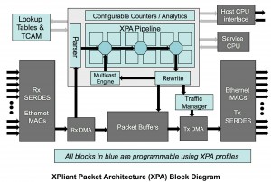
imageMicrosoft Azure Networking has ported its L3 Border Gateway Protocol (BGP) routing stack to Cavium XPliant switches.

This has been accomplished, the company says, through the use of the Switch Abstraction Interface (SAI), which enables portability and interoperability across different hardware platforms.

Historically switch silicon suppliers offered proprietary software interfaces requiring extensive software porting by customers to create an end user switch product. This resulted in a proprietary lock-in for these legacy switch silicon suppliers.

The SAI was defined as an abstraction interface for switching Asics to remove these barriers.

SAI enables system developers to port software to the best switch silicon that supports these SAI abstractions.

Earlier this year Cavium announced SAI support in the XPliant switch SDK (software development kit),  software now released for general use. Microsoft has easily ported Layer 3 BGP routing applications to the XPliant switch SDK based on the SAI interface.

“SAI adoption will enable customers to seamlessly deploy multiple vendors’ silicon into the network,” says Microsoft’s Kamala Subramaniam.

Cavium’s XPliant Ethernet switch family targets applications in cloud / enterprise data centers and service provider infrastructure, for both top-of-rack and backbone applications with bandwidths up to 3.2 Terabits per second in monolithic silicon support 1G, 10G, 25G, 40G, 50G and 100G interfaces.

This family of switches will also provide connectivity solutions for embedded applications.

david manners

Smart-meter IC market worth $1.2bn

smart meter IETSmart-meter chips were worth $1.2 billion last year, says IHS, at an ASP of $11. They went into 132 million meters.

“The semiconductor industry for electric meters is moving toward a single-chip solution for measuring and communicating with the grid station, which is an important industry trend to watch,” says IHS’ Robbie Galoso. “Water and gas meters require fewer semiconductor components; however, they need extra semiconductors for sensing and battery management.”

ASPs are expected to increase as industry needs increase for 32-bit micro-controller units (MCUs), memory chips, single system-on-chip (SoC) solutions and other components used in secured communications and other applications.

“The movement from 8-bit MCUs to higher margin 32-bit MCUs is a key industry trend,” said Noman Akhtar, analyst for IHS Technology. “The integration of these higher function microcontroller units also requires additional capabilities, such as increased memory, which further increases manufacturing costs.”

Meters are evolving from those that merely register end-user usage, into machines that can be queried for on-demand data, upgraded remotely, shut off in case of emergency or non-payment and used for variable pricing.

Meters will require greater application complexity, better security, improved communication ability, enhanced remote control ability and higher resolution.

That means increased need for memory and system-on-chip (SoC) solutions with greater capabilities in a smaller package than in the past.

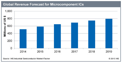
ihs-forecast-microcomponent

david manners