Author Archives: david manners

AMS to fab in New York

New York Governor Andrew Cuomo

New York Governor Andrew Cuomo

AMS CEO Kirk Laney

AMS CEO Kirk Laney

AMS is to fab wafers in New York under an innovative deal with the State.

A public-private funding deal will see New York State pay for the building of a fab designed to an AMS spec with AMS leasing and operating the fab for 20 years.

It will be an analogue fab of which the first stage will be an eight inch 130nm facility capable of 150k wafers a year with the possibility of expansion to 450k wafers per year.

The deal is structured so that it avoids AMS paying depreciation costs on the fab and equipment.

Over the 20 years lease, AMS is expected to spend $2 billion on the fab.

The fab will be built at the Marcy Nanocentre at Utica and will be the first fab to be built at Marcy which is owned by the SUNY Polytechnic Institute.

SUN Poly also owns the Nanotech Megaplex in Albany where GE is setting up a power electronics packaging facility focussed on SiC devices.

“The Mohawk Valley is beginning an economic revolution around nanotechnology,” said New York State Governor Andrew Cuomo when announcing the AMS and GE deals.

Construction of the 200/300mm AMS fab will start in the Spring of 2016 with first silicon out by the end of 2017.

The fab will create 700 full-time jobs and 500 jobs at contractors, sub-contractors, suppliers and partners.

See also: Photogallery – AMS analogue process fab

david manners

Vertical GaN transistors have 1kV blocking voltages

GaN-based transistors with blocking voltages over 1kV

GaN-based transistors with blocking voltages over 1kV

GaN-based transistors with blocking voltages over 1kV have been developed by researchers in Japan.

Low resistance resulting in reduced power consumption and heating have attracted researchers to study GaN systems for nanoelectronics. Previous work has focused on laterally oriented GaN and AlGaN transistors, which readily provide a high mobility and low resistance.

However these structures are limited in terms of the break-down and threshold voltage that can be achieved without compromising device size, which may make them unsuitable for automobile applications. Now Tohru Oka and colleagues at the Research and Development Headquarters for Toyoda Gosei have shown how they can overcome these limitations by adopting a vertically orientated transistor.

Previous work has already shown that in this orientation the breakdown voltage can be increased by increasing the drift region thickness without compromising the device size. However, so far these structures have still been limited in the blocking voltage that the device can withstand while maintaining a low on-resistance.

“We redesigned the thicknesses and doping concentrations of channel and drift layers to reduce the resistances of the epitaxial layers while maintaining a blocking voltage of over 1.2 kV,” says Oka.

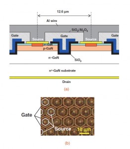
They also use hexagonally shaped trench gates to increase the gate width per unit area thereby reducing the specific on-resistance.

“These led to the excellent performance of 1.2kV-class vertical GaN MOSFETs with a specific on-resistance of less than 2mΩ cm2.”

david manners

IM aims rugged DRAM at automotive

IM launches robust DRAMs

IM launches robust DRAMs

Intelligent Memory (IM) has launched very robust DRAMs which withstand the highest operating temperatures and stress.

This is the first DRAM from anywhere to operate at 125°C and achieve grade 1 AEC-Q100 qualification, a company spokesman told Electronics Weekly

In applications such as automotive, avionic, aerospace and military applications, electronic components are often under extreme stress by rough environments such as hot temperatures or radiation. DRAM-memory ICs store data by holding an electric charge in little capacitors (the memory cells). High temperatures cause the leakage of the capacitors to increase rapidly, leading to transient single bit errors, also called soft-errors.

In addition, the DRAM cells tend to degradate quickly under stress, which further reduces the data-retention time of the cells, making it difficult to guarantee a soft-error-free long-term operation. Most manufacturers of automotive DRAM require a doubled or quadrupled refresh-rate to work against these physical limitations of DRAM cells.

Besides the fact that higher refresh-rates consume more power and generate more heat-dissipation, this method still covers a high risk due to the unknown degradation that may lead to random soft-errors only after weeks or months of use of the DRAM product.

Based on their ECC DRAM technology, Intelligent Memory now offers new DRAMs that can operate stable even at 125°C without the requirement to increase the refresh-rate. With their integrated Error Correction Code, I’M ECC DRAMs correct single-bit-errors caused by any kind of root-cause, such as heat, radiation or degradation. Also most bit-pattern-dependant bit-flips and even permanent single-bit hard-errors get covered by the on-chip ECC logic.

“IM is aiming to set new a standard for DRAM reliability for the safety-critical industry,” says IM’s Joseph Chan, “our eXtra Robustness ECC DRAMs (XR DRAM) have already proven their radiation-hardness. Now we want to show the automotive and avionic market that IM has the perfect solution for the increased demands of high operating temperature and reliability without any performance-loss. Our products are made for the markets that require long-term availability without revision shrinks.”

The new products with a temperature range of -40 to 125°C named “extreme Temperature” or “X-Grade” ECC DRAM are sampling now in DDR3 technology having a capacity of 1 Gigabit (part# IME1G16D3EEBG-15EX), with DDR2 and DDR1 products to follow later. AEC-Q100 Automotive Grade 1 qualified DDR3 parts are planned to be sampling by November 2015.

david manners

IM aims rugged DRAM at automotive

IM launches robust DRAMs

IM launches robust DRAMs

Intelligent Memory (IM) has launched very robust DRAMs which withstand the highest operating temperatures and stress.

This is the first DRAM from anywhere to operate at 125°C and achieve grade 1 AEC-Q100 qualification, a company spokesman told Electronics Weekly

In applications such as automotive, avionic, aerospace and military applications, electronic components are often under extreme stress by rough environments such as hot temperatures or radiation. DRAM-memory ICs store data by holding an electric charge in little capacitors (the memory cells). High temperatures cause the leakage of the capacitors to increase rapidly, leading to transient single bit errors, also called soft-errors.

In addition, the DRAM cells tend to degradate quickly under stress, which further reduces the data-retention time of the cells, making it difficult to guarantee a soft-error-free long-term operation. Most manufacturers of automotive DRAM require a doubled or quadrupled refresh-rate to work against these physical limitations of DRAM cells.

Besides the fact that higher refresh-rates consume more power and generate more heat-dissipation, this method still covers a high risk due to the unknown degradation that may lead to random soft-errors only after weeks or months of use of the DRAM product.

Based on their ECC DRAM technology, Intelligent Memory now offers new DRAMs that can operate stable even at 125°C without the requirement to increase the refresh-rate. With their integrated Error Correction Code, I’M ECC DRAMs correct single-bit-errors caused by any kind of root-cause, such as heat, radiation or degradation. Also most bit-pattern-dependant bit-flips and even permanent single-bit hard-errors get covered by the on-chip ECC logic.

“IM is aiming to set new a standard for DRAM reliability for the safety-critical industry,” says IM’s Joseph Chan, “our eXtra Robustness ECC DRAMs (XR DRAM) have already proven their radiation-hardness. Now we want to show the automotive and avionic market that IM has the perfect solution for the increased demands of high operating temperature and reliability without any performance-loss. Our products are made for the markets that require long-term availability without revision shrinks.”

The new products with a temperature range of -40 to 125°C named “extreme Temperature” or “X-Grade” ECC DRAM are sampling now in DDR3 technology having a capacity of 1 Gigabit (part# IME1G16D3EEBG-15EX), with DDR2 and DDR1 products to follow later. AEC-Q100 Automotive Grade 1 qualified DDR3 parts are planned to be sampling by November 2015.

david manners

Rugged DRAM from IM

IM launches robust DRAMs

IM launches robust DRAMs

Intelligent Memory (IM) has launched very robust DRAMs which withstand the highest operating temperatures and stress.

In applications such as automotive, avionic, aerospace and military applications, electronic components are often under extreme stress by rough environments such as hot temperatures or radiation. DRAM-memory ICs store data by holding an electric charge in little capacitors (the memory cells). High temperatures cause the leakage of the capacitors to increase rapidly, leading to transient single bit errors, also called soft-errors.

In addition, the DRAM cells tend to degradate quickly under stress, which further reduces the data-retention time of the cells, making it difficult to guarantee a soft-error-free long-term operation. Most manufacturers of automotive DRAM require a doubled or quadrupled refresh-rate to work against these physical limitations of DRAM cells.

Besides the fact that higher refresh-rates consume more power and generate more heat-dissipation, this method still covers a high risk due to the unknown degradation that may lead to random soft-errors only after weeks or months of use of the DRAM product.

Based on their ECC DRAM technology, Intelligent Memory now offers new DRAMs that can operate stable even at 125°C without the requirement to increase the refresh-rate. With their integrated Error Correction Code, I’M ECC DRAMs correct single-bit-errors caused by any kind of root-cause, such as heat, radiation or degradation. Also most bit-pattern-dependant bit-flips and even permanent single-bit hard-errors get covered by the on-chip ECC logic.

“IM is aiming to set new a standard for DRAM reliability for the safety-critical industry,” says IM’s Joseph Chan, “our eXtra Robustness ECC DRAMs (XR DRAM) have already proven their radiation-hardness. Now we want to show the automotive and avionic market that IM has the perfect solution for the increased demands of high operating temperature and reliability without any performance-loss. Our products are made for the markets that require long-term availability without revision shrinks.”

The new products with a temperature range of -40 to 125°C named “extreme Temperature” or “X-Grade” ECC DRAM are sampling now in DDR3 technology having a capacity of 1 Gigabit (part# IM1G16D3EEBG-15EX), with DDR2 and DDR1 products to follow later. AEC-Q100 Automotive Grade 1 qualified DDR3 parts are planned to be sampling by November 2015.

david manners

SEMI book-to-bill goes positive

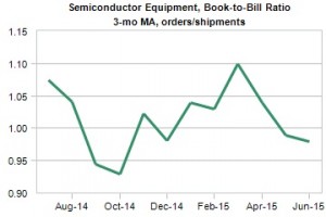
The SEMI book-to-bill went positive in July after a 0.98 in June and a 0.99 in May.

The SEMI book-to-bill went positive in July after a 0.98 in June and a 0.99 in May.

The SEMI book-to-bill went positive in July after a 0.98 in June and a 0.99 in May.

July’s ratio of 1.02 represented bookings of $1.59 billion and $1.56 billion of billings.

The $1.59 billion bookings figure is 5.1% higher than the final June 2015 level of $1.52 billion, and is 12.5% higher than the July 2014 order level of $1.42 billion.

The $1.56 billion billings figure is 0.3% higher than the final June 2015 level of $1.55 billion, and is 18.2% higher than the July 2014 billings level of $1.32 billion.

“Year-to-date, the bookings and billings reported in the SEMI North American equipment book-to-bill report indicate a solid year for the industry,” says SEMI CEO Denny McGuirk. “The outlook for the remainder of the year is somewhat clouded, but we see investments in 3D NAND and advanced packaging as drivers.”

The SEMI book-to-bill for April was 1.04, for March 1.1 and for February 1.03.

SEMI is a global industry association serving the nano- and micro-electronic manufacturing supply chains with 1,900 member companies.

The data contained in the report was compiled by David Powell, an independent financial services firm.

See alsoSEMI book-to-bill languishes


david manners

LAPIS sampling 10-cell li-ion battery monitoring IC

LAPIS is sampling a 10-cell lithium-ion battery monitoring LSI that provides a current consumption of 25μA

LAPIS is sampling a 10-cell lithium-ion battery monitoring LSI that provides a current consumption of 25μA

LAPIS Semiconductor, a part of ROHM, is sampling a 10-cell lithium-ion battery monitoring LSI that provides a current consumption of 25μA (typ.) making it suitable for battery protection systems in cordless vacuum cleaners, electric tools, and other portable equipment.

The ML5233 has 0.1μA (typ.) current consumption during power down, minimising the effects on battery capacity – even during long-term storage – and contributing to more eco-friendly products with virtually no loss of charged battery power.

In addition, built-in temperature and short-circuit current detection circuits enable detection of not only over-charge/discharge and overcurrent, but also abnormal (high) temperatures during discharge along with battery pack short-circuits – all without an MCU. This decreases footprint by 20% and reduces the number of external components from four to one, leading to smaller battery protection systems and lighter development load.

Overcharge detection accuracy (±15mV per each cell) increases charging efficiency by 7% over products with ±50mV accuracy.

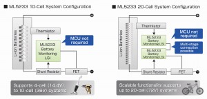
High-voltage processes support 4-10 cells in series using a single LSI, ensuring compatibility with electric tools and other equipment in the 14V to 36V range.

Two LSIs can be combined to support up 20 cells in series and up to 72V.

The company writes:

The ML5233 is a protection IC for the 4- to 10-cell Li-ion rechargeable battery pack. It detects individual cell overvoltage/undervoltage and the pack overcurrent/over-temperature, and then automatically controls the ON/OFF state of the external charge/discharge NMOS-FETs accordingly. Also the ML5233 can be cascaded to handle battery packs with more than 10 cells.

See also: French firm wins Lapis Semi Bluetooth antenna design in


david manners