Author Archives: david manners

FTDI Chip launches evaluation modules for next-gen USB technology

To encourage the widespread use of its next generation USB interfacing technology, FTDI Chip has unveiled a new family of evaluation/development modules. image

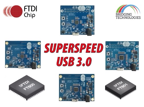
The company’s FT600/1Q USB 3.0 SuperSpeed ICs, which are already in full volume production, are forthwith backed up by the UMFT60XX offering.

This module family is made of 4 models, which provide different FIFO bus interfaces and data bit widths. Through these modules operational parameters of FT600/1Q devices can be fully assessed and interfacing with external hardware undertaken, such as FPGA platforms from the industry’s leading suppliers.

Measuring 78.7mm x 60mm, the UMFT600A and UMFT601A each have a high speed mezzanine card (HSMC) interface with 16-bit and 32-bit wide FIFO buses respectively.

Qvers the same functionality in relation to Xilinx boards.

Fully compatible with USB 3.0 SuperSpeed (5Gbits/s), USB 2.0 High Speed (480Mbits/s) and USB 2.0 Full Speed (12Mbits/s) data transfer, the UMFT60xx modules support 2 parallel slave FIFO bus protocols with an achievable data burst rate of around 400MBytes/s. The multi-channel FIFO mode can handle up to 4 logic channels. It is complemented by the 245 synchronous FIFO mode, which is optimised for more straightforward operation.

“We recognized early on that USB 3.0 system designs that are reliant on programmable logic, rather than MCU technology, are going to have a multitude of important benefits to the embedded engineering fraternity. They will allow bill-of-materials costs to be kept under control and the writing/compiling of masses of C code to be avoided,” states Fred Dart, CEO and founder of FTDI Chip. “As a result we have worked closely with the most prominent companies in the programmable sector to promote this more technologically and financial efficient method of implementing USB 3.0. The new modules we have introduced are designed such that they can plug into most FPGA development platforms supplied by vendors such as Xilinx or Altera.”

david manners

Power semiconductor market to grow at 5%

The overall power semiconductor market, including both power discretes and power modules, is predicted to grow 5% in 2015 to reach $17 billion, says IHSimage.

In 2014, y-o-y power discrete revenue grew 5% and power module revenue grew 12%.

The global power module market is projected to comprise nearly one third (30 percent) of the power semiconductor market by 2019, growing at twice the rate of power discretes, from 2014 to 2019, says IHS.

“OEMs will continue to want modular power solutions, which can be integrated easily into various subsystems and used in many different devices,” says IHS’ Richard Eden, “power modules are widely found in inverters for wind converters, photovoltaic solar energy systems and other renewable energy applications. They are also found in industrial motor drives and hybrid and electric vehicles.”

Infineon continued to be the largest supplier for the global power semiconductor market in 2014, with an estimated market share of 13%. Mitsubishi ranked second, at 7%. ST moved up to the third market position, displacing Toshiba, with an estimated market share of 6%.

With the acquisition of IR by Infineon last year, the market landscape for power semiconductors is changing. The merged companies held almost 27% of the power transistor market in 2014.

The transistor product category includes bipolar transistors, metal-oxide semiconductor field-effect transistors (MOSFETs), and insulated-gate bipolar transistor (IGBT) products, accounting for about two thirds of the total discrete power semiconductor market.

Mitsubishi Electric was the largest supplier for power modules in 2014, although the company’s estimated share of the market remained at 24% for 2013 and 2014. Infineon maintained the second-ranked position at 20%.

The top four power module suppliers – Mitsubishi, Infineon, Semikron and Fuji Electric – accounted for 65% of the global power module market in 2014.

david manners

Toshiba adds high luminous flux GaN-on-Si LEDs

Toshiba has added four GaN-on-Si LEDS to its TL1L4 series which provide a high luminous flux and are suited to applications ranging from street and stadium lighting to LED light bulbs and down lighting for use in the home. imageAll offer a colour rendering index of Ra70 min. and a typical forward voltage of 2.8V.

Like the existing members of the TL1L4 series, GaN-on-Si technology has been used to create LEDs optimised for both output and energy efficiency.

However, the new 4A5B type improves upon these existing products by providing a luminous flux of 140lm (min at 85°C) compared to 130lm (min).

The products make it possible to meet the market demands for improved lighting fixture efficacy by achieving efficacies of over 110lm/W in a finished luminaire – with Toshiba assuming 90% driver efficiency, 90% optical efficiency, and junctions at 85°C.

Measuring 3.5 x 3.5mm, with a lens-top, the LEDs offer differing correlated colour temperatures (CCTs), with the TL1L4-DW0 providing 6,500K, the TL1L4-NT0 providing 5,700K, the TL1L4-NW0 5,000K and the TL1L4-WH0 4,000K.

See alsoImec extends GaN-on-Si R&D programme

More Toshiba stories on Electronics Weekly »


david manners

Intepro launches auto-ranging power source

Intepro of Sandhurst, the power ATE specialist, has introduced an Auto-Ranging Programmable DC Power Source.

Model PSI 9000 provides up to 15kW in 3U rack-mount chassis. The auto-ranging feature maintains full rated power output at lower-voltage settings; units can be paralleled up to 150kW

A single 3U chassis houses up to 15kW of DC power and can be paralleled up to 150 kilowatts. Each chassis features a controller that allows the flexibility of separating into individual sources or paralleling for high-power applications.

Intepro launches auto-ranging power source

Intepro launches auto-ranging power source

A feature of the PSI 9000 Series is its auto-ranging output. Unlike DC sources that provide rated power only when maximum voltage is applied to the load, the auto-ranging output stage is capable of delivering three times higher output current at reduced voltages.

This feature is especially useful when testing products that require varied input voltages while maintaining regulated output power. With auto-ranging, a single-system provides a complete test solution compared to buying multiple sources to address low- and high-voltage/current requirements.

The PSI 9000 Series features an interactive touch panel menu navigation system that simplifies set up and storing to test profiles. The industry leading high-efficiency unit (up to 95.5%) includes an integrated true function generator. Complex test sequences can be loaded from and saved to a standard USB flash drive. The unit also includes simulations for PV (photovoltaic) arrays and fuel cells.

“The PSI 9000 Series is designed to simplify test set up and operation,” said Gerard Sheehan, Intepro’s CTO, “Front panel controls include an intuitive LCD display and control knobs for setting voltage, current, power or internal resistance simulation values.”

Additional features of the RoHS-compliant PSI 9000 Series include: a galvanically isolated analog interface for voltage, current and power programming and monitoring, digital plug-and-play modules supporting RS232, Ethernet, CANopen, Modbus TCP, Profibus, Devicenet and IEEE/GPIB, and SCPI command language support.

The PSI 9000 Series is offered in models with output power ratings of 0-3.3kW, 0-5kW, 0-10kW and 0-15kW in a single 3U chassis. The PSI 9000 3U family includes eight voltage models ranging to 1,500VDC.

david manners

Diamond Microwave adds to GaN PA range

Diamond Microwave of Leeds, the high performance microwave power amplifiers specialist, has announced a ten-fold increase in its power output capability with the addition of a 1kW X-band model to the company’s range of GaN-based pulsed solid-state power amplifiers (SSPAWimage).

The DMX1K001 is an ultra-compact SSPA operating over a 1200MHz bandwidth centred at 9.5GHz. The ultra-compact design measures only 244 x 134 x 50mm3 excluding heatsink and connectors, making it ideally suited for use as an alternative to a travelling wave tube amplifier (TWTA) in various radar applications.

“Like all our GaN SSPAs, these amplifiers are extremely compact, employing a chip-and-wire microwave design,” said Ian Davis, business development manager at Diamond Microwave. “This state-of-the art performance is combined with a power-to-volume ratio we believe to be among the highest in the industry for such products. Similar designs can be tailored to suit other frequency ranges in the 1-18GHz range.”

The Diamond Microwave amplifier range features designs that are flexible in layout and architecture, and are fully customisable to meet individual specifications for electrical, mechanical and environmental parameters. All of Diamond Microwave’s amplifiers are suited to demanding defence, aerospace and communications applications.

david manners

Quantenna sampling 10G Wave 3 WiFi for 10Gbps

Quantenna is sampling 10G Wave 3 Wi-Fi products built on Quantenna’s True 8×8 QSR10G Wi-Fi platform with multi-user MIMO (MU-MIMO) technology for home wireless access points and residential gateways.

Quantenna’s up-to-12-streams 10G Wave 3 can address both the service provider and retail market segments.

10G Wave 3 WiFi supports speeds up to 10Gbps attained by combining True 8×8 MIMO configuration for 5GHz networks with a 4×4 MIMO configuration on 2.4GHz networks for a combined 12-stream configuration.

Sam Heidari - Quantenna CEOQuantenna’s 10G Wave 3 platform delivers the maximum capacity within the minimum spectrum so that more streams can be simultaneously transmitted with improved range and reliability.

This means that 802.11 Wi-Fi access points or gateways using 10G Wave 3 can support more clients, each running more efficiently for such demanding applications as real-time video, OTT video, voice, IoT and other services.

Single-user MIMO (SU-MIMO), 1×1 and 2×2 client performance is also improved, ensuring that the millions of currently shipping mainstream smart phones, tablets and notebook PCs will also benefit from an improved Wi-Fi experience.

The QSR10G Wave 3 product family also supports a unique adaptive MIMO architecture. This enables 10G Wave 3 access points to maximize overall network performance, delivering the best possible capacity across all client devices. This is important as the mix of legacy and new client devices are changing, as end consumers adopt more devices with 802.11ac.

Key Wave 3 features and Benefits
• Integrated AP chipset for dual-band (5GHz and 2.4GHz), dual concurrent operation and management
• 160MHz channel support for 5GHz networks. When combined with 8×8 MIMO configuration, this offers 4x the capacity of 80MHz 4×4 MIMO networks
• Unique adaptive MIMO configuration
• Up to 1024 QAM modulation for 2.4GHz and 5GHz transmissions
• Supports rich set of interfaces to external hosts such as PCIe Gen3/Gen2, RXAUI, RGMII, and others

The QSR10G product family delivers 10G Wi-Fi with up to 8×8 MU-MIMO for smart access points, wireless cable/DSL gateways. Key features of the industry’s first 10G Wave 3 Wi-Fi product family include:

• QSR10GU
o Peak PHY rate of near 10Gbps
o Support for simultaneous 5GHz and 2.4GHz networks
o 12 stream operation
• QSR10GA
o Peak PHY rate of 9Gbps
o Support for simultaneous 5GHz and 2.4GHz networks
o 10 stream operation
• QSR10PA
o Peak PHY rate of 7Gbps
o Support for simultaneous 5GHz and 2.4GHz networks
o 8 stream operation
• QSR10G5
o Peak PHY rate of 8.6Gbps
o Support for 5GHz networks
o 8 stream operation

“In Wi-Fi access points more antennas are always better, but 10G Wave 3 is not just about 8×8 MU-MIMO and faster speeds. It’s about making better use of network and airtime efficiency to support the growing number of connected devices, services and applications,” said Dr. Sam Heidari, Quantenna CEO.

david manners

ADI launches clock jitter attenuator for base-stations

Today ADI introduced a clock jitter attenuator designed to support the JESD204B serial interface standard for connecting high-speed data converters and FPGAs operating in base station designs.

The JESD204B interface was developed to address high-data rate system design needs, and the 3.2-GHz HMC7044 clock jitter attenuator contains functions that support and enhance the unique capabilities of that interface standard.

ADI HMC7044 block diagram

ADI HMC7044 block diagram

The HMC7044 delivers 50-fs jitter performance, which improves the signal-to-noise ratio and dynamic range of high-speed data converters, and the device provides 14 low-noise and configurable outputs that provide flexibility in interfacing with many different components.

The HMC7044 also offers a wide range of clock management and distribution features that make it possible for designers of base stations to build an entire clock design with a single device.

In base stations applications there are many serial JESD204B data converter channels that require their data frames to be aligned with an FPGA. The HMC7044 clock jitter attenuator simplifies JESD204B system design by generating source-synchronous and adjustable sample and frame alignment (SYSREF) clocks in a data converter system.

The device features two phase-locked loops (PLLs) and overlapping, on-chip, voltage-controlled oscillators (VCOs). The first PLL locks a low-noise, local voltage-controlled clock oscillator (VCXO) to a relative noisy reference, while the second PLL multiplies the VCXO signal up to the VCO frequency with exceptionally little added noise.

For cellular infrastructure JESD204B clock generation, wireless infrastructure, data converter clocking, microwave baseband cards and other high-speed communications applications, the architecture of the HMC7044 offers excellent frequency generation performance with low phase noise and integrated jitter.

HMC7044 Clock Jitter Attenuator Key Features

• JEDEC JESD204B support
• Ultra-low RMS jitter: 50 fs (12 KHz to 20 MHz, typical)
• Noise floor: -162 dBc/Hz at 245.76 MHz
• Low phase noise: < -142 dBc/Hz at 800 kHz to 983.04 MHz output frequency
• Up to 14 device differential device clocks from PLL2
• External VCO input supports up to 5 GHz
• On-board regulators

The device costs $12.75 in a 10-mm × 10-mm LFCSP package

david manners

ADI launches clock jitter attenuator for base-stations

Today ADI introduced a clock jitter attenuator designed to support the JESD204B serial interface standard for connecting high-speed data converters and FPGAs operating in base station designs.

The JESD204B interface was developed to address high-data rate system design needs, and the 3.2-GHz HMC7044 clock jitter attenuator contains functions that support and enhance the unique capabilities of that interface standard.

The HMC7044 delivers 50-fs jitter performance, which improves the signal-to-noise ratio and dynamic range of high-speed data converters, and the device provides 14 low-noise and configurable outputs that provide flexibility in interfacing with many different components.

The HMC7044 also offers a wide range of clock management and distribution features that make it possible for designers of base stations to build an entire clock design with a single device.

In base stations applications there are many serial JESD204B data converter channels that require their data frames to be aligned with an FPGA. The HMC7044 clock jitter attenuator simplifies JESD204B system design by generating source-synchronous and adjustable sample and frame alignment (SYSREF) clocks in a data converter system.

The device features two phase-locked loops (PLLs) and overlapping, on-chip, voltage-controlled oscillators (VCOs). The first PLL locks a low-noise, local voltage-controlled clock oscillator (VCXO) to a relative noisy reference, while the second PLL multiplies the VCXO signal up to the VCO frequency with exceptionally little added noise.

For cellular infrastructure JESD204B clock generation, wireless infrastructure, data converter clocking, microwave baseband cards and other high-speed communications applications, the architecture of the HMC7044 offers excellent frequency generation performance with low phase noise and integrated jitter.

HMC7044 Clock Jitter Attenuator Key Features

• JEDEC JESD204B support
• Ultra-low RMS jitter: 50 fs (12 KHz to 20 MHz, typical)
• Noise floor: -162 dBc/Hz at 245.76 MHz
• Low phase noise: < -142 dBc/Hz at 800 kHz to 983.04 MHz output frequency
• Up to 14 device differential device clocks from PLL2
• External VCO input supports up to 5 GHz
• On-board regulators

The device costs $12.75 in a 10-mm × 10-mm LFCSP package

david manners

Infineon GaN on SiC RF power transistors anticipate 5G

Infineon is sampling under NDA its first devices in a family of GaN on SiC RF power transistors. The devices allow manufacturers of mobile base stations to build smaller, more powerful and more flexible transmitters.

With higher efficiency, improved power density and more bandwidth than currently used RF power transistors, the new devices improve the economics of building cellular infrastructure and pave the way for the transition to 5G.

Infineon GaN on SiC RF power transistors anticipate 5G

Infineon GaN on SiC RF power transistors anticipate 5G

The devices leverage the performance of GaN technology to achieve 10% higher efficiency and 5x the power density of LDMOS transistors commonly. This translates to smaller footprints and power requirements for the PAs of base station transmitters which operate in either the 1.8-2.2 GHz or 2.3-2.7 GHz frequency range. Future GaN on SiC devices will also support 5G cellular bands up to the 6 GHz frequency range.

Design flexibility and support for the next-generation of 4G technology are additional benefits of GaN devices for RF power applications. The new devices have twice the RF bandwidth of LDMOS, so that one PA can support multiple operating frequencies. They also have increased instantaneous bandwidth available for transmitters, which lets a carrier offer higher dates using the data aggregation technique specified for 4.5G cellular networks.

Read more Infineon Technologies on Electronics Weekly »


david manners