Author Archives: david manners

Xilinx ships 16nm finfet FPGA

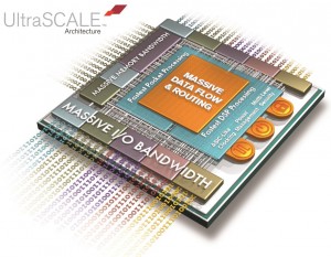
Xilinx has made its first customer shipment of 16nm finfet FPGAs,

Xilinx ships 16nm finfet FPGA

Xilinx ships 16nm finfet FPGA

“We call this a “Three-Peat”, says Xilinx vice-president Victor Peng. “Being first to market with products at 28nm, 20nm, and now at 16nm.”

The Zynq UltraScale+ multiprocessor SoC (MPSoC), built on TSMC’s 16FF+ process, enables the development of embedded vision, ADAS, I-IoT and communications systems by providing 5X system-level performance/watt and any-to-any connectivity.

“TSMC’s ongoing collaboration with Xilinx has resulted in the early shipment of a world class 16nm Finfet multiprocessing SoC,” says TSMC’s  BJ Woo. “Xilinx and TSMC have delivered industry-leading silicon performance with the lowest power consumption, and highest level of systems integration and intelligence among programmable logic products.”

david manners

VR in sight for ARM’s Mali T-880

VR in sight for ARM's Mali T-880

VR in sight for ARM’s Mali T-880

ARM is positioning its top-end graphics IP – the Mali T-880 – as a virtual reality (VR) engine.

“Smartphones are as big as we want them to be but more computational power is needed in the graphics and display to get more realism,” Mark Dickinson, ARM’s graphics general told electronics Weekly. “We want quality of pixels not quantity of pixels.”

Although VR has been touted as an imminent killer app for the past 30 years, ARM believes that computing power is now capable of delivering it.

“VR is very dependent on computational power,” said Dickinson. “Head-sets need a high frame-rate to handle panning, resolution needs to be high, there has to be a different image for each eye and there’s a need for very low latency.”

ARM, via its T-880 Mali graphics engine launched earlier this year, is able to deliver all of those, said Dickinson.

“We have a solution to VR on the smartphone,” he said. “Smartphone manufacturers are
seeing VR as one of the use cases.”

Asked when smartphone manufacturers would put VR into their phones, Dickinson replied: “They already have done,” citing the Samsung Galaxy S6 and the Samsung Galaxy Note 4.

ARM can actually boast of a VR design win – the Samsung Gear VR uses ARM’s Mali graphics for its VR effects.

david manners

Semiconductor inventories steady, says Jewell

Semiconductor inventories steady, says Jewell

Semiconductor inventories steady, says Jewell

Despite alarm about the state of semiconductor inventories, particularly from the foundries, Bill Jewell’s Semiconductor Intelligence says that: “Semiconductor inventories appear to be under control throughout the semiconductor device supply chain.”

At the semiconductor manufacturers inventory ratios have been stable for eighteen months, says Jewell

Exceptions are Intel and Qualcomm where lower revenues caused Intel’s inventory ratio to go from 29% in Q2 2014 to 37% in Q2 2015 while Qualcomm’s ratio went from 24% to 41% in the same period.

Jewell then looked at users, taking six of the top eight purchasers of semiconductors. None showed any significant change in inventory rate compared to this time last year.

So how about the disties? Jewell finds that the inventory ratio at Arrow and Avnet has been close to 40% for the last eight years.

Finally there are the EMS companies where Jewell surveyed Jabil, Sanmina, Flextronics and Celestica. He finds that the EMS inventory ratio hit 55% in 2007 and has been “fairly steady” since, with a rise in 2011 to 57% from a 50% ratio in 2011.

david manners

ST digital division faces guillotine

The French business weekly magazine Challenges reports that the future of ST’s digital division is now in the hands of President Francois Hollande.image

The French Economics Minister and the Defence Minister have reviewed the possible divestment or closure of Crolles, the Finance Ministry has had its say, the CFE-CGC union has been to see Hollande’s advisers and now the decision on what to do rests with the President.

The magazine reports that ST CEO Carlo Bozotti is accused, in a report by the Direction générale des entreprises (DGE) de Bercy, of sabotaging the digital division by publicly referring to its “unacceptable losses” – remarks which are alleged to have caused customers to freeze contracts, so further weakening the division and adding to the justification for closing it.

At stake are 2,500 jobs at Crolles and the last vestige of European-controlled access to advanced semiconductor production.

There are various proposed scenarios – sale or closure of the entire site involving 2,500 jobs, a reduction in jobs by between 1,000 and 1,200 people, or a reduction to a rump of only 300.

However there are warnings that a big hit at Crolles could affect another 20,000 jobs in the Grenoble region.

ST management is criticised for “supporting the share price at the expense of investment planning for the future.” ST is said to have spent $2.6 billion on dividends between 2005 and 2014 while the company has made losses of $3.6 billion. Last year it paid out $354 million to shareholders while losing $465 million.

Arguments for keeping Crolles going are the importance of the military not having to rely on American components and the opportunity presented by FD-SOI for providing leadership in IoT and connected cars.

France and Italy have 27.5% stakes in ST but waived their dividends to provide resources for investment. Italian government sources are staying schtum on the issue of the digital division.

david manners

FTDI Chip boosts EVE ecosystem

FTDI Chip has enlarged the development ecosystem surrounding its Embedded Video Engine (EVE) platform for advanced human machine interface (HMI) implementation.

The latest additions concern the FT810 series of high resolution EVE ICs, which are now in full scale production. In order to support these devices, the company has announced the VM810C50 family of compact development modules. They extend the functionality offered by the VM800C family that accompanies the FT800 series, so that large higher clarity imagery can be rendered and faster data transfer rates benefitted from.

The VM810C50A-D features a 5.0-inch TFT display with WVGA (800×480 pixel) resolution and a resistive touchscreen. Conversely, for the VM810C50A-N, the display is not included.

Instead, through use of its 40-pin FFC interface, a suitable 4.3/5.0-inch LCD (with SVGA, WVGA, VGA, WQVGA or QVGA resolutions and a 4-wire resistive touch screen interface) may be attached. This means that the appropriate display can be chosen and subsequently connected.

Both of these credit card sized units act as SPI slaves connecting to the specified system microcontroller through their single SPI interfaces.

They each have a built-in micro speaker, audio power amplifier, 3-stage audio filter, an audio line out option and LCD backlight control.

Power can be drawn for these modules via either the 2.0mm power jack, the USB Micro-B port or SPI interface. The SPI interface supports 5V tolerant buffers when using a 5V SPI supply.

The FT810 EVE devices from FTDI Chip combine touch, display and audio functionality on a single chip and employ the innovative approach to HMI implementation that has been pioneered by the company. Here images, templates, overlays, fonts and sounds are treated as objects.

Using this object-orientated methodology, graphics can be rendered line-by-line at 1/16th pixel resolution, as opposed to pixel-by-pixel.

This streamlines implementation, allowing marked reductions in cost, board real estate and system complexity. The FT810 and other members of the FT81x series are able to work with displays of up to 800×600 pixels.

They have 18-bit or 24-bit RGB interfacing options, plus 1Mbytes of RAM capacity for storing graphics data. A built-in JPEG decompression engine provides better graphics data usage and enables more effective HMI implementation.

These devices support multiple colour palettes of 16-bits and 32-bits with transparency. Their SPI interfaces support 30MHz operation.


david manners

Memsstar raises funding to boost exports

Memsstar, the Livingston manufacturer of MEMS manufacturing equipment has secured a imagesignificant funding deal with Santander supported by a guarantee from UK Export Finance.

Memsstar makes etch and deposition systems for MEMS manufacturing. It also represents SMEs in a range of European funding programmes.

Memsstar exports around 90% of its products and is looking to capitalise on this momentum in key markets.

The business currently has an annual turnover of circa £8 million but is targeting to grow this to £13 million over the next two years.

“This will provide the company with a source of working capital to enable the ongoing development of our customer base and ensure that we remain competitive for our existing customers,” says the company’s CFO Keith Rutter.

“This is a great example of how a government guarantee can work alongside a trade specialist bank to help a leading, innovative UK firm,” says Jonathan Leonard of UK Export Finance.

david manners

Plessey raises £30m to expand GaN-on-Si LED manufacturing

Plessey is to carry out a major expansion of the company’s LED manufacturing facility in Plymouth, after securing a £30 million loan from Deutsche Bank. image

The £60 million expansion will provide the base for new solid state lighting technologies and products, increasing the Company’s production capabilities by a factor of 30, more than tripling its workforce to about 535 employees and positioning Plessey to capture a significant share of the multi-billion dollar, and growing, solid state lighting market.

Plessey’s MaGIC GaN-on-Silicon technology can cut the cost of LED lighting by using standard silicon manufacturing techniques instead of sapphire-based manufacturing.

“Deutsche Bank is providing us with a senior secured term loan facility that meets our financial needs for the next three to five years,” says Plessey CFO Iain Silvester, “the bank has come up with a progressive flexible facility that supports our expansion plans for our manufacturing capacity here in Plymouth. Plessey will increase its manufacturing capacity from over 100 million square millimetres of Gallium Nitride material per year to more than 3 billion square millimetres. The facility modifications, which are also supported by £6.7 million from the Regional Growth Fund, will take place during 2015, with additional manufacturing tools and facilities coming on stream through the end of this year through to 2017. During this time we expect about 400 new jobs to be created.”

Michael LeGoff, Plessey’s CEO added: “We are entering a very exciting period for the company with our new technology and products now gaining traction in one of the fastest growing technology markets, solid state lighting. The expansion is highly significant for the Company but also for British high-tech manufacturing,” says Plessey CEO Michael LeGoff, “it aligns well with national strategies, such as the Growth Review, that support manufacturing and make the UK a global leading exporter of high value goods.”

david manners

Socionext in volume production of camera engine supporting new sensor functions

Socionext, the Fujitsu-Panasonic SoC jv, is in volume production of a camera front engine specialized for Bayer data processing that supports the latest sensors.socio

The MB86S29 is a Milbeaut Image Processor aimed at smartphones. By supporting the latest image sensors, the MB86S29 lets module makers implement these functions without replacing their application processors.

Recently, it is common to find cameras in smartphones or other mobile devices that are configured with application processors (AP) equipped with built-in image signal processor (ISP) functionalities. These APs can directly process output from image sensors, and help reduce the footprint and cost of camera modules.

The MB86S29 supports this trend as a “Camera Front Engine” that replaces conventional ISPs. Connected in between an image sensor and an AP, it is specialized for Bayer data processing, so users can configure their APs with the same interface directory connected to image sensors, and to make full use of phase detect auto focus (AF) or high dynamic range (HDR).

The MB86S29 has 4 lanes each of 2.1Gbps MIPI Rx / Tx. It can process 16M pixel images at 30 frame per second (fps). It is also applicable for noise reduction, shading correction, and 3A (AE / AF / AWB) detection. It is available in the smallest package of any member of the Milbeaut series, at 4mm x 4mm.

Since its first release in 2000, the Milbeaut series of image processors has established a track record in applications from digital SLR cameras for prosumers to commodities like smartphones, or industrial equipment like security cameras. Socionext will continue to deliver a broad range of imaging solutions, based on its technological expertise and a long history of providing services to its customers.

The MB86S29 has been designed to utilize “Hybrid AF”, which combines the accuracy of contrast AF and the speed of phase detect AF, enabling maximum 4x faster AF, in comparison with the previous Milbeaut products.

The MB86S29 also supports Sensor HDR. Conventional HDR imaging, which generates a picture from multiple frames taken with different exposures, has disadvantages, such as images blurs caused by the difference between the frames, and time needed to take those multiple frames. The MB86S29 can process data with different exposure settings within one image so it can process the HDR images with higher visibility in 16M pixel, at the speed of 30 fps.

□ MB86S29 Specifications
・ 16M Pixel at 30fps, Bayer Output
・ Compatible with phase detect AF Sensors
・ Compatible with Sensor HDR
・ Defective Pixel Correction (including pixels for phase detect AF)
・ Shading Correction
・ Package: 4mm x 4mm
・ MIPI-Rx: 4 lanes (2.1Gbps) + 2 lanes (1.5Gbps)
・ MIPI-Tx: 4 lans (2.1Gbps)
・ Dual ARM processor Core

TheMB86S29 costs $3 when purchased in volume quantities of 5 Million pieces or more.

david manners

Optical memory chip

A team of researchers have produced an optical memory IC

A team of researchers have produced an optical memory IC

A team of researchers from the Karlsruhe institute of Technology and the Universities of Oxford, Munster and Exeter have produced an optical memory IC.

“We have demonstrated a robust, non-volatile, all-photonic memory based on phase-change materials,” say the researchers, “by using optical near-field effects, we realize bit storage of up to eight levels in a single device that readily switches between intermediate states.”

The chip’s memory cells feature single-shot readout and switching energies as low as 13.4 pJ at speeds approaching 1 GHz. Individual memory elements can be addressed using a wavelength multiplexing scheme.

“Our multi-level, multi-bit devices provide a pathway towards eliminating the von Neumann bottleneck and portend a new paradigm in all-photonic memory and non-conventional computing,” say the team.

david manners

Bad Q3 for Taiwan foundries

Q3, traditionally the industry’s strongest quarter, will not be a good quarter for the Big Three tsmc 427Taiwanese foundries, reports Digitimes Research.

The combined revenues of TSMC, UMC and VIS (Vanguard International Semiconductor) will be 0.8% down q-o-q and 3.7% down y-o-y.

Q3 revenues are expected to be $8.03 billion compared to Q2’s $8.09 billion and the $8.33 billion of Q3 2014.

The turndown would have been worse were it not for a rise in ASPs due to an increase in the proportion of advanced (sub45nm) processes in the the mix.

Digitimes notes that TSMC started to record 16nm revenues for the first time in Q3.

See also: TSMC forecasts sales fall

See alsoSmartphone demand collapse hits foundries

Read more TSMC stories on Electronics Weekly »

david manners